|
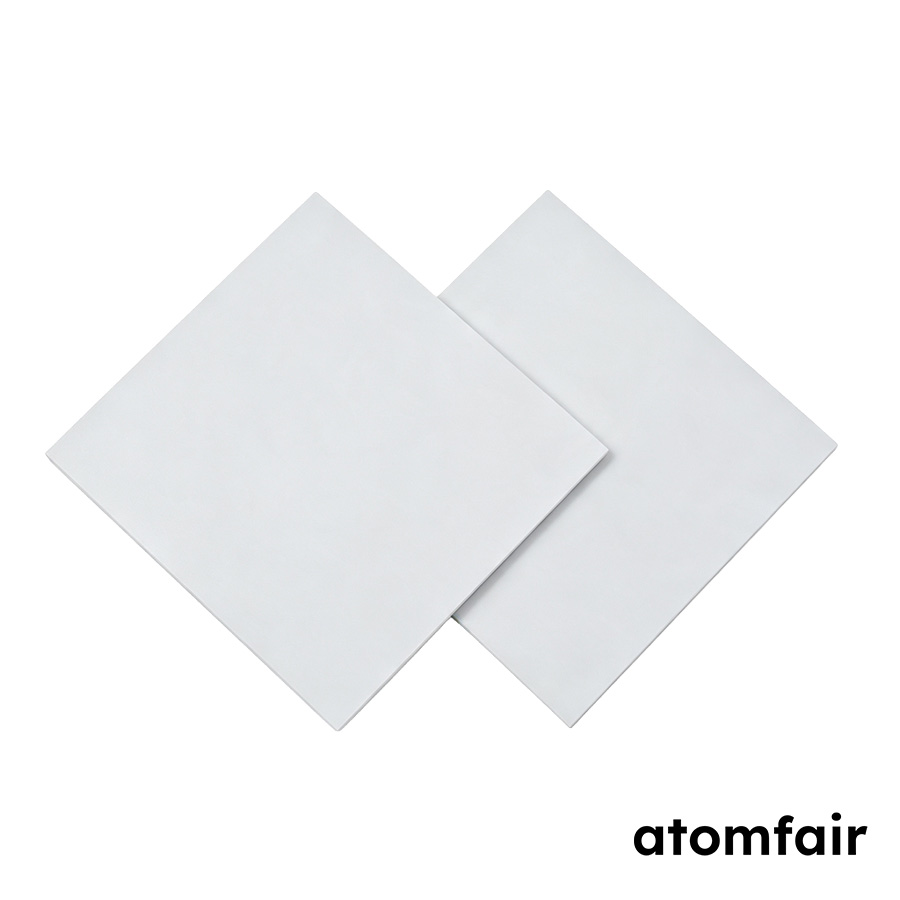
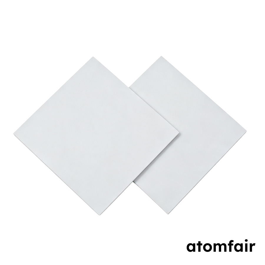
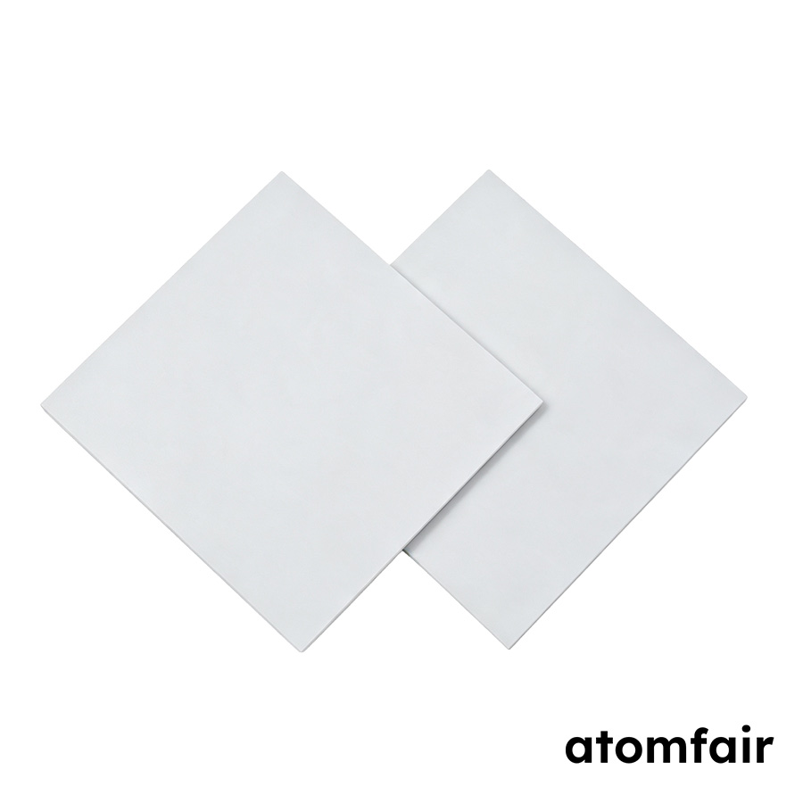
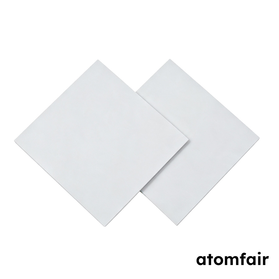
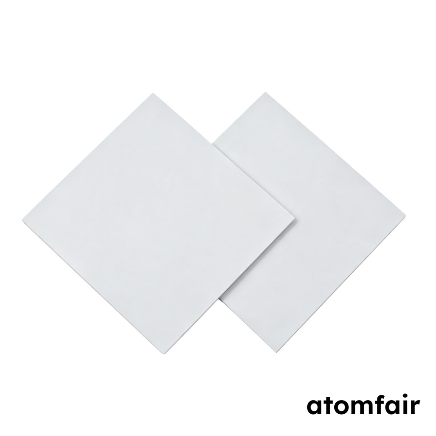
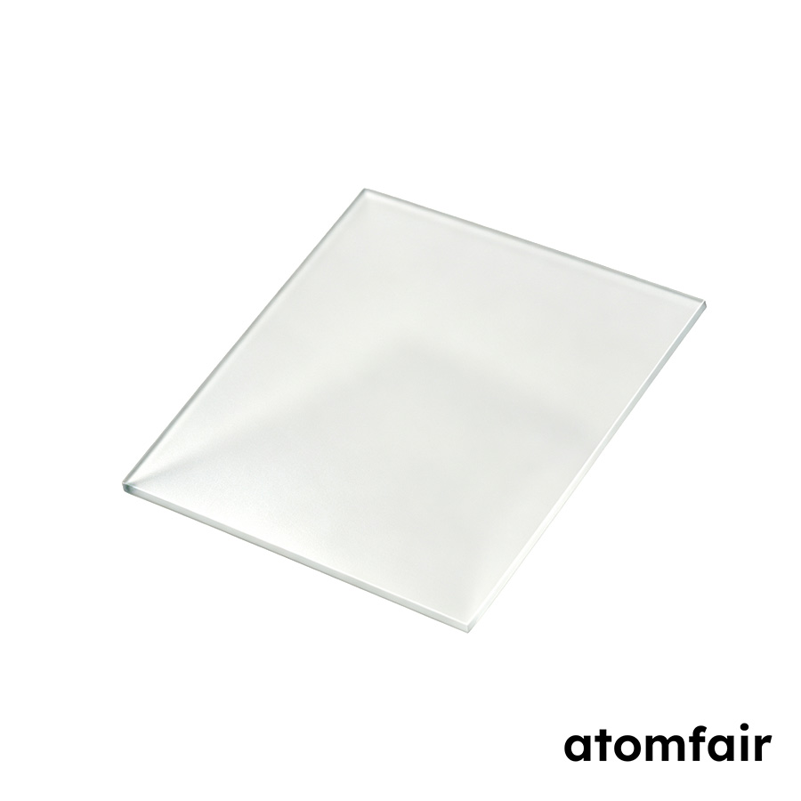
Lanthanum Aluminate Single Crystal Substrate, (110), DSP (10 pcs/box)
Product Type: LaAlO3 single crystal substrate
Research-grade laboratory product
|
|||||||||||||||||||||||||||||||||||||||||||||||||||
|
|||||||||||||||||||||||||||||||||||||||||||||||||||
|
LABORATORY PROCUREMENT SUPPORT
For material matching, specification review, model selection or configuration confirmation, contact our technical sales team.
E-MAIL: inquiry@atomfair.com
|
|||||||||||||||||||||||||||||||||||||||||||||||||||
|
Manufacturer: Atomfair LLC
Brand: ATOMFAIR®
|
The substrate exhibits chemical stability in mineral acids at room temperature but dissolves in phosphoric acid above 150°C. Thermal expansion mismatch with deposited films may induce stress or cracking during high-temperature processing.
- Chemical Stability Constraint: Avoid exposure to phosphoric acid at temperatures exceeding 150°C to prevent substrate dissolution.
- Thermal Expansion Mismatch: Account for the substrate's thermal expansion coefficient of 9.4 × 10⁻⁶ /°C when designing annealing or deposition cycles to minimize film-substrate stress.
- Twin Domain Presence: Polished substrates contain natural twin domains that may affect epitaxial film uniformity and require consideration in device fabrication.
- Orientation Tolerance: Confirm the ±0.5° orientation tolerance is compatible with the crystallographic alignment requirements of the target thin-film process.
Inspect the substrate for surface defects and confirm orientation before loading into the deposition chamber. Clean the substrate surface using a standardized solvent sequence to remove organic residues without attacking the material.
Required Equipment: Optical microscope or surface inspection system, Cleanroom-grade tweezers (PTFE or ceramic), Solvent rinse station (acetone, isopropanol, deionized water), Nitrogen blow gun or spin dryer
- Inspect substrate surface
Inspect the polished substrate under an optical microscope for scratches, chips, or particulate contamination before any processing step. - Clean substrate surface
Rinse the substrate sequentially in acetone, isopropanol, and deionized water to remove organic residues and particulate matter. - Dry substrate completely
Dry the substrate with a stream of filtered nitrogen or in a spin dryer to prevent water spot formation. - Mount substrate in deposition holder
Mount the clean, dry substrate onto the deposition stage or sample holder, ensuring secure contact to maintain thermal uniformity during processing. - Preheat substrate to deposition temperature
Set the deposition chamber to the target temperature, accounting for the substrate's 9.4 × 10⁻⁶ /°C thermal expansion rate. - Initiate thin-film deposition
Begin the deposition process once the substrate temperature and chamber vacuum have stabilized within the process parameters.
How do the natural twin domains in LaAlO3 (110) substrates affect thin-film epitaxy?
The natural twin domains present in polished LaAlO3 substrates can influence the crystallographic orientation of deposited films. According to the product specification, the substrate has a pseudo-cubic crystal structure with lattice constant a = 3.792 Å and orientation tolerance ±0.5°. Twin domains may create local variations in surface symmetry, which should be considered when growing highly oriented or lattice-matched epitaxial layers.
What chemical etching method is recommended for LaAlO3 substrates?
LaAlO3 is insoluble in mineral acids at room temperature but can be etched in H3PO4 above 150°C. This information is provided in the product's technical specifications, indicating that hot phosphoric acid is the appropriate etchant for substrate cleaning or patterning.
What are the dielectric properties of LaAlO3 (110) substrates at cryogenic temperatures?
The dielectric constant of LaAlO3 is 24.6, and the loss tangent is approximately 3 × 10⁻⁴ at 300 K and 0.6 × 10⁻⁴ at 77 K. These values, stated in the product specifications, are critical for evaluating substrate suitability in microwave and cryogenic electronic applications.
The LaAlO3 (110) DSP substrate offers high thermal stability (melting point 2080°C) and low dielectric loss at cryogenic temperatures (loss tangent ~0.6×10⁻⁴ at 77 K), making it suitable for microwave and epitaxial applications. The inherent natural twin domains and annealing-dependent color variation require careful consideration for process uniformity.
Positive
- High thermal stability and low dielectric loss: With a melting point of 2080°C and loss tangent ~0.6×10⁻⁴ at 77 K, this substrate is suitable for high-temperature and cryogenic microwave applications.
- Chemical stability to common acids: Insoluble in mineral acids at room temperature, allowing standard wet processing without degradation.
Trade-offs
- Natural twin domains present: Polished substrates exhibit natural twin domains, which may affect the uniformity of epitaxial films and require careful characterization.
- Appearance variability with annealing: The material color ranges from brown-yellow to brown depending on annealing condition, indicating potential optical property variation.
Every advanced material, component, equipment, and instrument in our catalog is backed by rigorous testing. We maintain strict internal quality management frameworks and align with CE conformity metrics to deliver transparent, reproducible performance data via our public open-science repository.
To request raw batch performance data, submit formal vendor registration paperwork, or execute a fast-turnaround R&D manufacturing loop, contact us at inquiry@atomfair.com.
Item is dispatched under the Atomfair Shipping & Delivery Framework (Free worldwide shipping on orders over $59 USD excl. heavy equipment). Return is governed by the Atomfair Return & Refund Policy (7-day technical return window).