|
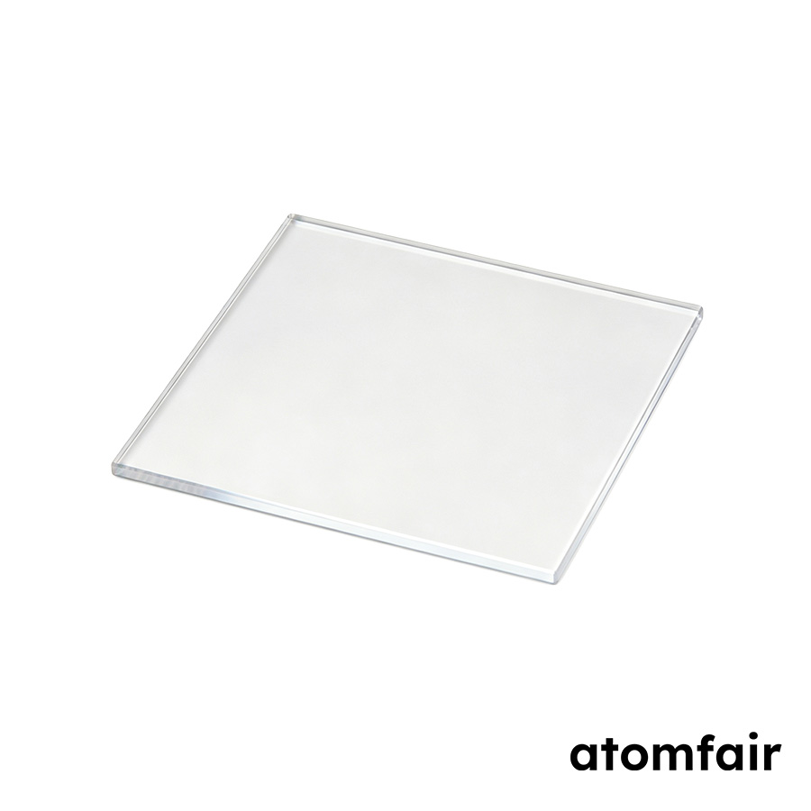
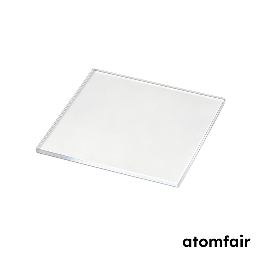
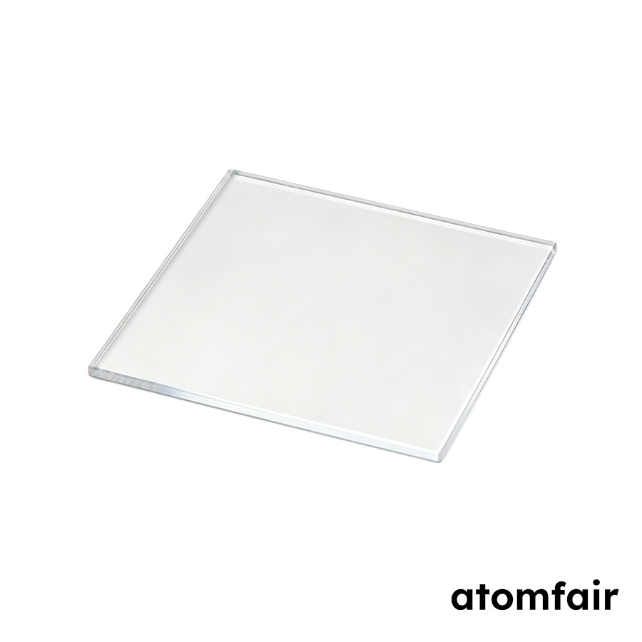
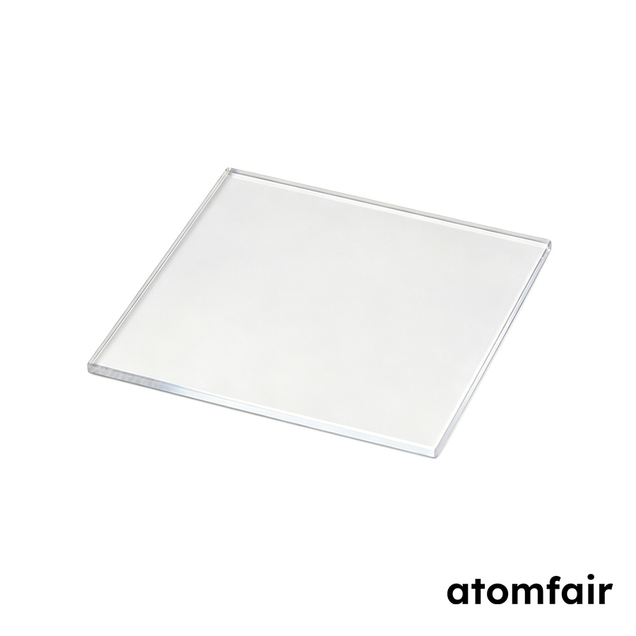
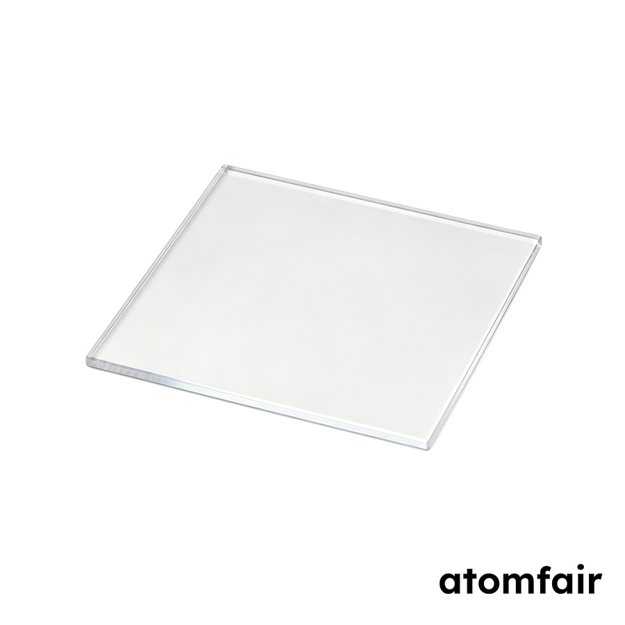
JGS2 Quartz glass Substrate – 2 inch (50.8 mm), 10 pcs/box
Product Type: Glass substrate
Research-grade laboratory product
|
|||||||||||||||||||||||||||
|
|||||||||||||||||||||||||||
|
PRODUCT SELECTION SUPPORT
For model selection, material matching or specification support, contact our technical sales team.
E-MAIL: inquiry@atomfair.com
|
|||||||||||||||||||||||||||
|
Manufacturer: Atomfair LLC
Brand: ATOMFAIR®
|
How do the surface roughness, flatness, and scratch-dig specifications of the JGS2 quartz glass substrate impact its suitability for thin film deposition and optical coating applications?
The specified surface roughness (Ra <0.5 nm), flatness (<5 μm), and Scratch/Dig 40/20 ensure minimal scattering and high uniformity, making the substrate well-suited for thin film deposition, optical coatings, and photolithography. These parameters are critical for achieving consistent film thickness and low defect density in high-precision optical and electronic devices. The JGS2 quartz material is a standard choice for demanding optical substrate applications.
What is the significance of the 16 mm flat orientation on the 2-inch JGS2 quartz glass substrate for alignment in semiconductor processing equipment?
The 16 mm flat provides a mechanical reference for rotational alignment, enabling repeatable positioning in photolithography, spin-coating, and other wafer processing equipment. This flat orientation is standard for 2-inch substrates and ensures that multiple substrates can be consistently oriented for batch processing. The flat length of 16 mm is compatible with alignment notches in manual and automated handling systems.
What are the recommended handling and storage practices to maintain the Ra <0.5 nm surface roughness and Scratch/Dig 40/20 quality of the JGS2 quartz glass substrate?
To preserve the specified surface quality, the substrates should be handled in a cleanroom environment using clean gloves or tweezers, and stored in the original box to avoid dust and scratches. The package of 10 pcs/box provides a protective environment for storage and transport. Any cleaning or processing should follow standard quartz substrate protocols to avoid degrading the scratch-dig rating.
The JGS2 quartz glass substrate (2 inch, 10 pcs/box) provides Ra <0.5 nm roughness and <5 um flatness for precision optical use, but the 500 um thickness necessitates careful handling to prevent mechanical damage.
Positive
- Sub-nanometer surface roughness: Ra <0.5 nm ensures minimal light scattering, making the substrate suitable for high-resolution optical and lithographic applications.
- Tight flatness tolerance: <5 um flatness across the 2-inch diameter minimizes wavefront distortion in interferometry, photolithography, and precision optics.
Trade-offs
- Thin substrate fragility: 500 um thickness makes the substrate mechanically delicate; breakage risk is elevated during handling, mounting, or thermal cycling.
Every advanced material, component, equipment, and instrument in our catalog is backed by rigorous testing. We maintain strict internal quality management frameworks and align with CE conformity metrics to deliver transparent, reproducible performance data via our public open-science repository.
To request raw batch performance data, submit formal vendor registration paperwork, or execute a fast-turnaround R&D manufacturing loop, contact us at inquiry@atomfair.com.
Item is dispatched under the Atomfair Shipping & Delivery Framework (Free worldwide shipping on orders over $59 USD excl. heavy equipment). Return is governed by the Atomfair Return & Refund Policy (7-day technical return window).