ATOMFAIR® IN-SITU RAMAN CELLS & HIGH-PRECISION PEEK BATTERY MOLDS KITRESEARCH GRADE HARDWARE
|
|||||||||||||||||||||||
|
|||||||||||||||||||||||
|
TAILORED SOLUTIONS FOR RESEARCH
Contact our laboratory hardware division for specialized configuration parameters or official pricing quotes.
EMAIL: inquiry@atomfair.com
|
|||||||||||||||||||||||
|
Manufacturer: Atomfair LLC
Brand: ATOMFAIR®
|
Optical window cleanliness and mechanical compression limits are critical to avoid signal distortion and component damage. Electrolyte compatibility with PEEK and internal alloy parts must be verified to ensure long-term structural stability.
- Optical Window Maintenance: Clean optical windows only with recommended spectroscopic solvents to prevent contamination and loss of signal fidelity.
- Compression Limit Adherence: Do not exceed the specified mechanical compression limits during solid-state sample preparation to avoid permanent deformation or failure.
- Electrolyte Compatibility Check: Select electrolytes that are compatible with PEEK and internal alloy components to prevent corrosion or chemical attack.
- Leak-Proof Sealing Requirement: Ensure complete sealing of the cell assembly to prevent electrolyte leakage and eliminate short-circuit paths.
- Dielectric Insulation Use: Properly install dielectric insulation rings to maintain electrical isolation under high pressure and avoid short circuits.
This guide covers the essential preparation and assembly steps for reliable in-situ spectroscopic measurements. Follow these steps to avoid hardware damage and maintain data integrity.
Required Equipment: Recommended spectroscopic cleaning solvent
- Clean Optical Windows
Inspect and clean the quartz/sapphire optical windows using a lint-free cloth wetted with the recommended spectroscopic solvent. - Assemble Constant-Spacing Mold
Assemble the PEEK mold with the constant-spacing control mechanism and dielectric insulation rings to ensure uniform electrode contact. - Apply Mechanical Compression
Apply mechanical compression to the mold assembly within the specified limit to secure the solid-state sample without causing damage. - Seal and Connect Cell
Seal the cell assembly completely to guarantee leak-proof operation, then connect it to the potentiostat and Raman spectrometer for measurement.
How does the constant-spacing mechanism in the PEEK molds improve in-situ Raman data quality compared to standard compression cells?
The constant-spacing assembly mechanics provide absolute thickness regulation over the electrolyte/pellet matrix, ensuring uniform physical contact. This eliminates sample variations that can distort spectroscopic signals, allowing for more accurate real-time observation of electrode surface changes during cycling.
Are the in-situ Raman cells compatible with both aqueous and non-aqueous electrolytes?
Yes, the cells feature corrosion-resistant internal alloy parts that are compatible with various non-aqueous and aqueous liquid electrolytes. Additionally, the leak-proof structural design ensures stable long-term operation across different electrolyte chemistries.
What are the recommended handling procedures for the optical viewports and compression steps in the ATOMFAIR in-situ Raman kit?
Optical viewports must be cleaned only with recommended spectroscopic solvents to maintain clean optical paths. During solid-state sample preparation, do not exceed the specified mechanical compression limits to avoid damaging the mold or causing short circuits.
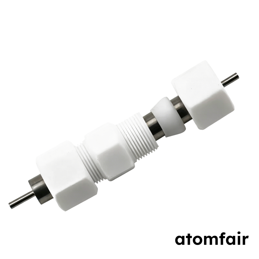
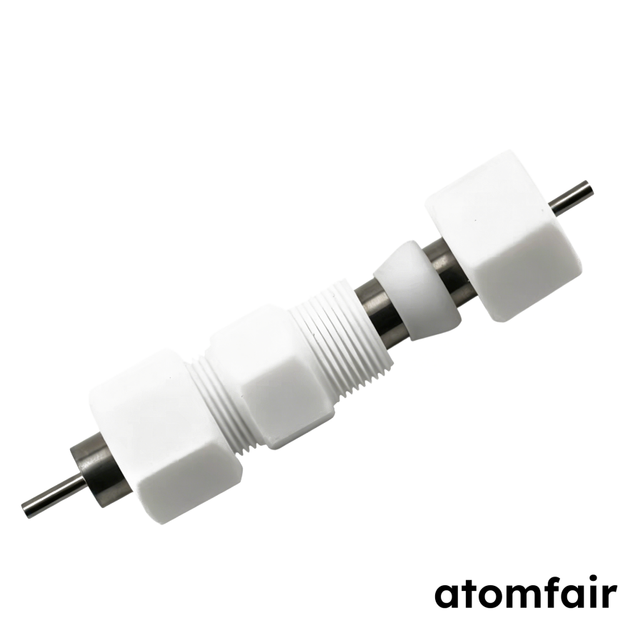
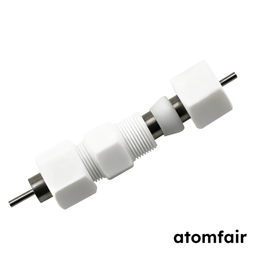
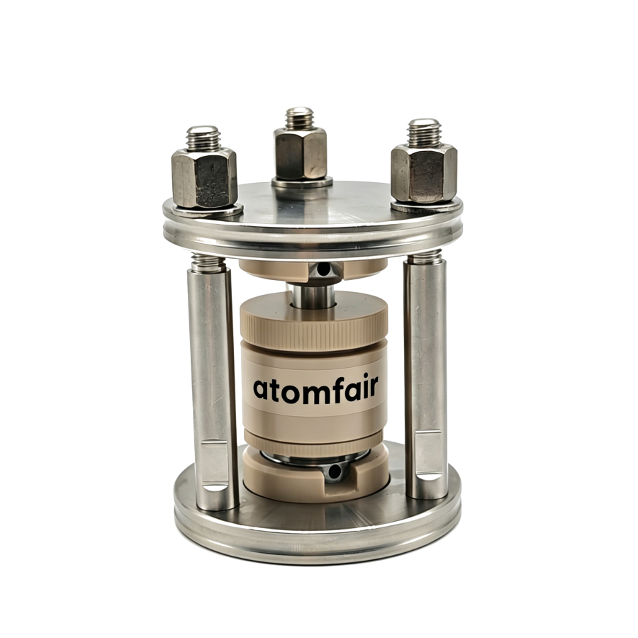
This kit integrates two in-situ Raman cells with Quartz/Sapphire viewports and two high-precision PEEK constant-spacing molds, enabling real-time spectroscopic analysis of electrode materials during charge-discharge cycling with uniform thickness control and high-pressure short-circuit protection.
Positive
- Optimized optical ports for signal acquisition: The integrated Quartz/Sapphire viewports provide clean laser entry and maximize backscatter signal collection, preventing peak distortion during in-situ Raman measurements.
- Constant-spacing mechanism for uniform contact: The built-in constant-spacing assembly ensures absolute thickness regulation of the electrolyte/pellet matrix, enabling reproducible physical contact and eliminating sample variation.
Trade-offs
- Requires specific solvent cleaning: Optical windows must be maintained strictly with recommended spectroscopic solvents to avoid contamination and preserve signal integrity; improper cleaning can degrade performance.
- Mechanical compression limits enforced: During solid-state sample preparation, users must not exceed specified mechanical compression limits to prevent damage to the PEEK molds or internal components.
Every advanced material, component, equipment, and instrument in our catalog is backed by rigorous testing. We maintain strict internal quality management frameworks and align with CE conformity metrics to deliver transparent, reproducible performance data via our public open-science repository.
To request raw batch performance data, submit formal vendor registration paperwork, or execute a fast-turnaround R&D manufacturing loop, contact us at inquiry@atomfair.com.
Item is dispatched under the Atomfair Shipping & Delivery Framework (Free worldwide shipping on orders over $59 USD excl. heavy equipment). Return is governed by the Atomfair Return & Refund Policy (7-day technical return window).