|
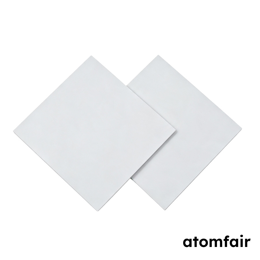
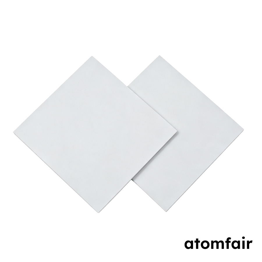
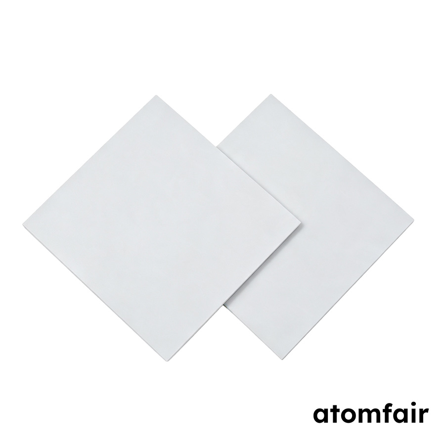
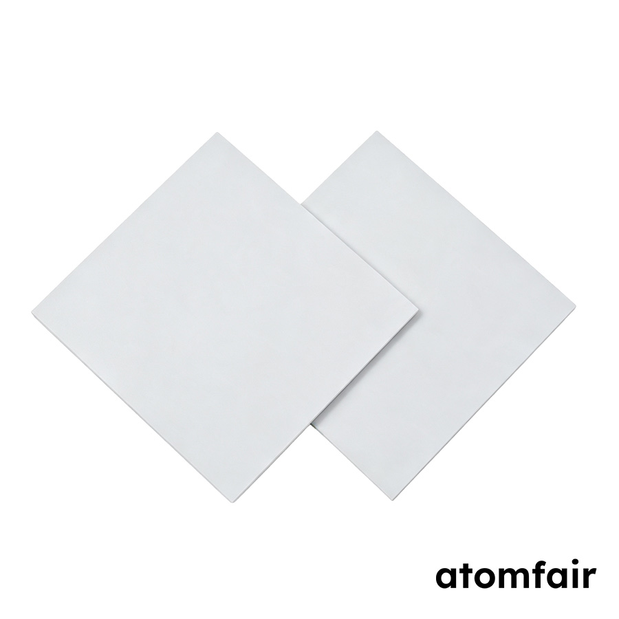
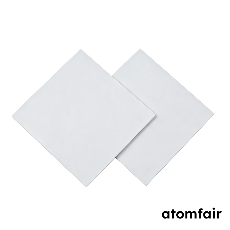
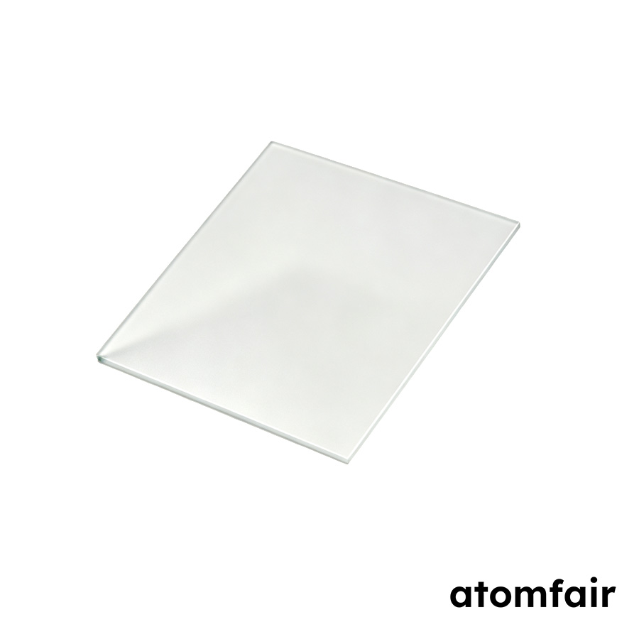
Yttria-Stabilized Zirconia Single Crystal Substrate, (110), SSP (10 pcs/box)
Product Type: YSZ single crystal substrate
Research-grade laboratory product
|
|||||||||||||||||||||||||||||||||||||||||||||||
|
|||||||||||||||||||||||||||||||||||||||||||||||
|
LABORATORY PROCUREMENT SUPPORT
For material matching, specification review, model selection or configuration confirmation, contact our technical sales team.
E-MAIL: inquiry@atomfair.com
|
|||||||||||||||||||||||||||||||||||||||||||||||
|
Manufacturer: Atomfair LLC
Brand: ATOMFAIR®
|
What is the significance of the (110) orientation for YSZ single crystal substrates from Atomfair?
The (110) orientation provides a specific surface atomic arrangement that is critical for epitaxial growth of thin films requiring in-plane anisotropy. The substrates are supplied with an orientation tolerance of ±0.5°, ensuring consistent crystallographic alignment across the entire substrate. This precision is essential for reproducible device fabrication in oxide thin-film research.
How does the thermal expansion coefficient of YSZ substrates affect thin-film deposition processing?
YSZ has a thermal expansion coefficient of 10.3 × 10⁻⁶ /°C, which is relatively high compared to many common thin-film materials. This mismatch must be accounted for during deposition and cooling to avoid thermal stress and delamination. The substrate's melting point of 2800°C allows high-temperature annealing steps without degradation, making it suitable for demanding oxide film growth processes.
What are the available substrate dimensions and how do they influence experimental setup?
Two specification options are available: 10 × 10 × 0.5 mm and 5 × 5 × 0.5 mm, both sharing the same (110) orientation and SSP surface finish with roughness < 5 Å. The 0.5 mm thickness provides mechanical rigidity for handling and sample holders while maintaining low thermal mass for rapid heating. Size selection primarily depends on sample holder compatibility and the desired thin-film deposition area.
YSZ (110) single crystal substrate with 99.99% purity, <5 Å surface roughness, and 2800°C melting point, available in two size options (10×10×0.5 mm and 5×5×0.5 mm), suitable for high-temperature epitaxial thin-film deposition.
Positive
- High purity and atomically smooth surface: 99.99% crystal purity and surface roughness <5 Å provide a clean, flat template for epitaxial growth, minimizing defect nucleation at the substrate-film interface.
- Exceptional thermal stability: Melting point of 2800°C and a thermal expansion coefficient of 10.3×10⁻⁶/°C enable the substrate to withstand high-temperature processing steps common in oxide thin-film and solid-oxide fuel cell research.
Trade-offs
- Limited dimensional options: Only two standard sizes (10×10×0.5 mm and 5×5×0.5 mm) are available, which may restrict sample geometry for experiments requiring larger or non-standard footprints.
- Orientation tolerance requires alignment verification: Orientation tolerance of ±0.5° demands careful mounting and alignment during deposition to avoid off-axis growth effects, particularly for lattice-matched heterostructures.
Every advanced material, component, equipment, and instrument in our catalog is backed by rigorous testing. We maintain strict internal quality management frameworks and align with CE conformity metrics to deliver transparent, reproducible performance data via our public open-science repository.
To request raw batch performance data, submit formal vendor registration paperwork, or execute a fast-turnaround R&D manufacturing loop, contact us at inquiry@atomfair.com.
Item is dispatched under the Atomfair Shipping & Delivery Framework (Free worldwide shipping on orders over $59 USD excl. heavy equipment). Return is governed by the Atomfair Return & Refund Policy (7-day technical return window).