|
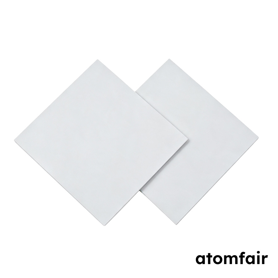
Sapphire Substrate – 4 inch (100 mm) A-Plane Single-Side Polished
Product Type: Sapphire substrate
Research-grade laboratory product
|
|||||||||||||||||||||||||||||||||||||
|
|||||||||||||||||||||||||||||||||||||
|
PRODUCT SELECTION SUPPORT
For model selection, material matching or specification support, contact our technical sales team.
E-MAIL: inquiry@atomfair.com
|
|||||||||||||||||||||||||||||||||||||
|
Manufacturer: Atomfair LLC
Brand: ATOMFAIR®
|
What are the TTV, BOW, and WARP specifications for the 4-inch A-Plane sapphire substrate?
The TTV is <10 µm, BOW is <10 µm, and WARP is <15 µm as specified for the 4-inch (100 mm) A-Plane single-side polished sapphire substrate from Atomfair.
What are the front-side and back-side surface roughness specifications for this sapphire substrate?
The front-side roughness is Epi-ready with Ra <0.3 nm, while the back-side roughness is fine ground with Ra <1.2 µm, as stated in the product specifications.
What thickness options are available for the 4-inch A-Plane sapphire substrate?
The standard thickness is 650 ± 25 µm, and optional thicknesses include 225 µm, 430 µm, and 1000 µm, as listed in the technical specifications.
The 4-inch A-Plane single-side polished sapphire substrate offers high-purity monocrystalline Al2O3 with epi-ready front surface roughness below 0.3 nm, suitable for epitaxial growth. However, the back-side fine-ground finish and thickness tolerance of ±25 um impose additional handling and specification considerations for advanced applications.
Positive
- High-purity monocrystalline Al2O3: Material purity >99.99% minimizes impurity-related defects, which is critical for high-performance epitaxial and device fabrication processes.
- Epi-ready front-side roughness: Front-side roughness Ra <0.3 nm meets epi-ready standards, enabling direct use for thin film deposition without additional polishing steps.
Trade-offs
- Back-side fine-ground roughness: Back-side roughness Ra <1.2 um may require additional surface preparation for processes needing uniform thermal contact or back-side metallization.
- Thickness tolerance of ±25 um: The standard thickness tolerance of ±25 um can be a constraint for applications requiring precise optical path length or substrate resonance control.
Every advanced material, component, equipment, and instrument in our catalog is backed by rigorous testing. We maintain strict internal quality management frameworks and align with CE conformity metrics to deliver transparent, reproducible performance data via our public open-science repository.
To request raw batch performance data, submit formal vendor registration paperwork, or execute a fast-turnaround R&D manufacturing loop, contact us at inquiry@atomfair.com.
Item is dispatched under the Atomfair Shipping & Delivery Framework (Free worldwide shipping on orders over $59 USD excl. heavy equipment). Return is governed by the Atomfair Return & Refund Policy (7-day technical return window).