|
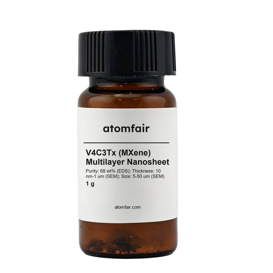
V4C3Tx (MXene) Multilayer Nanosheet, Package: 1 g
Product Type: MXene powder / nanosheet material
Research-grade laboratory product
|
|||||||||||||||||||
|
|||||||||||||||||||
|
LABORATORY PROCUREMENT SUPPORT
For material selection, specification confirmation and package-size quotation support, contact our technical sales team.
E-MAIL: inquiry@atomfair.com
|
|||||||||||||||||||
|
Supplier: Atomfair
Brand: ATOMFAIR®
|
Manufacturer: Atomfair LLC
Brand: ATOMFAIR®
How does the wide thickness range (10 nm–1 μm) of the V4C3Tx MXene multilayer nanosheet influence its performance in energy storage devices?
The 10 nm–1 μm thickness range (SEM) indicates a mixture of few-layer and multilayer flakes. Thinner flakes provide higher surface area and faster ion transport, while thicker flakes offer mechanical integrity. This polydispersity can lead to inconsistent electrode kinetics in supercapacitor or battery applications unless size-selection steps are employed.
What are the implications of the 68 wt% purity (EDS) for using this MXene in composite material development?
The 68 wt% purity (EDS) means the powder contains approximately 32 wt% residual phases, such as unetched MAX phase or oxide impurities. When incorporated into polymer or ceramic composites, these impurities can act as weak points or alter interfacial properties, potentially degrading mechanical or electrical performance. Purity should be confirmed before use in structural composites.
What storage and handling conditions are recommended to preserve the quality of the V4C3Tx MXene multilayer nanosheet powder?
The product description does not include specific handling or storage instructions for this V4C3Tx MXene powder. Users are advised to contact Atomfair at inquiry@atomfair.com for recommended conditions to avoid compromising the 68 wt% purity and 10 nm–1 μm thickness characteristics.
This V4C3Tx MXene multilayer nanosheet offers a broad thickness range (10 nm–1 µm) and lateral size distribution (5–50 µm) suitable for exploratory composite and electrode studies; however, its moderate purity (68 wt% by EDS) and SEM-based dimensional characterization introduce constraints for applications requiring high phase purity or statistically validated particle sizing.
Positive
- Wide thickness range: Thickness spans from 10 nm to 1 µm (SEM), enabling tunability for applications such as energy storage electrodes or EMI shielding where multilayer stack height influences performance.
- Broad lateral size distribution: Lateral flake size of 5–50 µm (SEM) provides flexibility for composite reinforcement or film formation where aspect ratio and percolation behavior are critical.
Trade-offs
- Moderate purity level: Purity is specified as 68 wt% by EDS; residual impurities may affect electrochemical behavior or require additional purification steps for high-sensitivity applications.
- SEM-based dimensional reporting: Thickness and size are measured by SEM without statistical distribution data; batch-to-batch variability in flake dimensions should be anticipated during process optimization.
Every advanced material, component, equipment, and instrument in our catalog is backed by rigorous testing. We maintain strict internal quality management frameworks and align with CE conformity metrics to deliver transparent, reproducible performance data via our public open-science repository.
To request raw batch performance data, submit formal vendor registration paperwork, or execute a fast-turnaround R&D manufacturing loop, contact us at inquiry@atomfair.com.
Item is dispatched under the Atomfair Shipping & Delivery Framework (Free worldwide shipping on orders over $59 USD excl. heavy equipment). Return is governed by the Atomfair Return & Refund Policy (7-day technical return window).