|
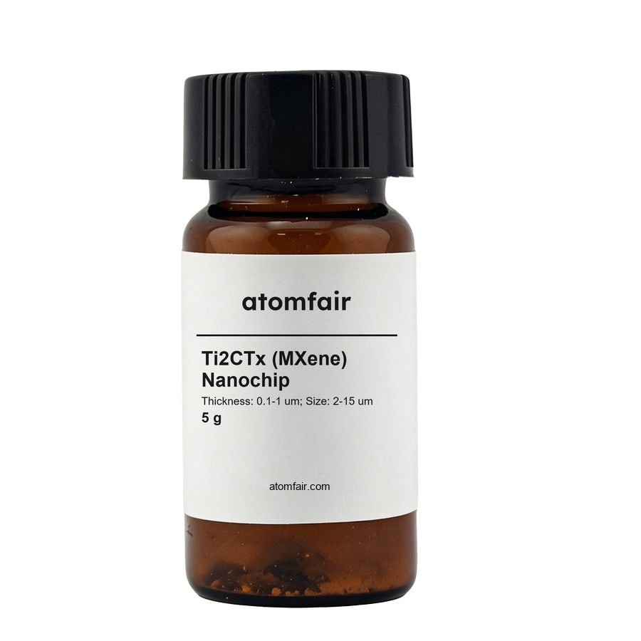
Ti2CTx (MXene) Nanochip, Package: 5 g
Product Type: MXene powder / nanosheet material
Research-grade laboratory product
|
|||||||||||||||||||
|
|||||||||||||||||||
|
LABORATORY PROCUREMENT SUPPORT
For material selection, specification confirmation and package-size quotation support, contact our technical sales team.
E-MAIL: inquiry@atomfair.com
|
|||||||||||||||||||
|
Supplier: Atomfair
Brand: ATOMFAIR®
|
Manufacturer: Atomfair LLC
Brand: ATOMFAIR®
What is the trade-off between thickness and lateral size in the Ti2CTx MXene Nanochip for achieving high aspect ratio?
The product offers thickness from 0.1 to 1 um and lateral size from 2 to 15 um. Thinner flakes (<0.5 um) combined with larger lateral sizes (>10 um) yield high aspect ratios desirable for film-based devices, while thicker flakes may be more robust for powder compaction. The polydisperse nature means a single batch contains a distribution, so users may need to fractionate for narrow aspect ratios.
What compatibility criteria should be verified when incorporating Ti2CTx MXene Nanochip into a device architecture?
Users must match the MXene composition (Ti2C), thickness range (0.1-1 um), and lateral size range (2-15 um) to their intended deposition or composite method. The product is supplied as a dry powder; compatibility with solvents, binders, or substrates is not pre-validated and should be tested under the specific processing conditions.
What storage and handling requirements apply to the Ti2CTx MXene Nanochip research-grade powder?
The material is a fine nanosheet powder with dimensions down to 0.1 um thickness and 2 um lateral size, requiring standard nanopowder precautions. It should be stored in a sealed, dry container under inert gas to prevent degradation. Handling should be conducted in a fume hood or glovebox with appropriate PPE to avoid inhalation and skin contact.
Evaluation of the Ti2CTx MXene nanochip (5 g) reveals well-specified lateral size and thickness ranges suitable for research-scale material studies, though the undefined termination chemistry and wide thickness spread introduce potential reproducibility challenges for precision applications.
Positive
- Controlled nanoscale thickness range: The product is specified with thickness 0.1-1 µm, allowing selection for size-dependent property studies.
- Defined lateral size distribution: Lateral dimensions of 2-15 µm provide consistent flake morphology for electrode fabrication or composite formulations.
Trade-offs
- Undefined surface termination composition: The Tx termination groups are not quantified; batch-to-batch variability in surface chemistry may affect electrochemical performance.
- Broad thickness distribution: The 0.1-1 µm thickness range spans an order of magnitude; applications requiring uniform layer thickness may need additional size sorting.
Every advanced material, component, equipment, and instrument in our catalog is backed by rigorous testing. We maintain strict internal quality management frameworks and align with CE conformity metrics to deliver transparent, reproducible performance data via our public open-science repository.
To request raw batch performance data, submit formal vendor registration paperwork, or execute a fast-turnaround R&D manufacturing loop, contact us at inquiry@atomfair.com.
Item is dispatched under the Atomfair Shipping & Delivery Framework (Free worldwide shipping on orders over $59 USD excl. heavy equipment). Return is governed by the Atomfair Return & Refund Policy (7-day technical return window).