|
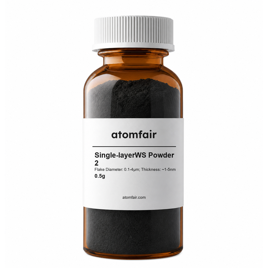
Single-layerWS Powder 2, 0.1-4μm, ~1-5nm, 0.5g
Product Type: 2D material powder
Research-grade laboratory product
|
|||||||||||||||||||
|
|||||||||||||||||||
|
LABORATORY PROCUREMENT SUPPORT
For material selection, specification confirmation and quotation preparation, contact our technical sales team.
E-MAIL: inquiry@atomfair.com
|
|||||||||||||||||||
|
Manufacturer: Atomfair LLC
Brand: ATOMFAIR®
|
What is the typical number of layers in Atomfair Single-layer WS2 Powder 2 given the stated thickness range of ~1–5 nm?
The product is labeled as single-layer WS2 powder, but the reported thickness range of ~1–5 nm spans beyond the theoretical monolayer thickness of ~0.6–0.7 nm, indicating that the powder likely contains a statistical mix of single-layer and few-layer flakes. The nominal flake diameter is 0.1–4 μm, and the thickness is ~1–5 nm, consistent with typical research-grade 2D material powders where the specification reflects the range across the batch.
What is the flake diameter distribution of Atomfair Single-layer WS2 Powder 2?
The flake diameter is specified as a range of 0.1–4 μm, indicating a broad distribution. The exact particle size distribution curve is not provided; the value is given for specification review and comparison. Researchers should confirm the required flake size for their application before ordering.
Atomfair Single-layer WS2 powder (SKU AF-NM-G-POWD-F143-0072) is supplied as a research-grade 2D material with specified flake diameter 0.1–4 μm and thickness ~1–5 nm in a 0.5 g package. The material is suitable for fundamental studies of tungsten disulfide monolayers, though the thickness range may include few-layer flakes.
Positive
- Single-layer WS2 powder: The product is explicitly supplied as single-layer tungsten disulfide powder, providing monolayer-thick flakes for advanced 2D material research in electronics and optoelectronics.
- Research-grade designation: The material is classified as a research-grade laboratory product, indicating it is prepared for experimental use and reproducibility in academic or industrial R&D settings.
Trade-offs
- Limited package size (0.5 g): The 0.5 g package size may be insufficient for large-scale experiments or multiple characterization runs, requiring multiple orders for extended studies.
- Thickness range may indicate few-layer stacks: The specified thickness of ~1–5 nm exceeds the theoretical monolayer thickness of WS2 (~0.6 nm), suggesting the material may contain few-layer flakes, which is a constraint for applications requiring strictly monolayer material.
Every advanced material, component, equipment, and instrument in our catalog is backed by rigorous testing. We maintain strict internal quality management frameworks and align with CE conformity metrics to deliver transparent, reproducible performance data via our public open-science repository.
To request raw batch performance data, submit formal vendor registration paperwork, or execute a fast-turnaround R&D manufacturing loop, contact us at inquiry@atomfair.com.
Item is dispatched under the Atomfair Shipping & Delivery Framework (Free worldwide shipping on orders over $59 USD excl. heavy equipment). Return is governed by the Atomfair Return & Refund Policy (7-day technical return window).