|
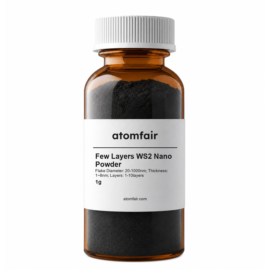
Few Layers WS2 Nano Powder, 20-1000nm, 1~8nm, 1g
Product Type: 2D material powder
Research-grade laboratory product
|
|||||||||||||||||||||
|
|||||||||||||||||||||
|
LABORATORY PROCUREMENT SUPPORT
For material selection, specification confirmation and quotation preparation, contact our technical sales team.
E-MAIL: inquiry@atomfair.com
|
|||||||||||||||||||||
|
Manufacturer: Atomfair LLC
Brand: ATOMFAIR®
|
What is the specified flake diameter range for this few-layer WS2 nano powder?
The flake diameter is specified as 20–1000 nm, as listed in the product specification table for Atomfair model AF-WS2-P1G. This range indicates that the powder contains a distribution of lateral sizes; the exact distribution within a given batch is not provided in the product data.
What is the specified layer count and thickness range for this few-layer WS2 nano powder?
The product is specified as having 1–10 layers with a corresponding thickness of 1–8 nm. Both parameters are provided as ranges; the exact number of layers and thickness per flake will vary within that range, and the correlation between the two is not explicitly defined in the product specification.
Few Layers WS2 Nano Powder with broad flake diameter (20-1000nm) and few-layer thickness (1-8nm, 1-10 layers) is evaluated for research applications requiring 2D material powder. The wide size distribution provides flexibility but requires careful characterization for consistent results.
Positive
- Broad flake diameter range: Flake diameter spans 20-1000nm, accommodating diverse experimental setups and integration requirements without the need for multiple source materials.
- Few-layer thickness control: Thickness of 1-8nm (1-10 layers) provides atomic-scale thinness, enabling studies of quantum confinement and surface-dominant phenomena in 2D WS2.
Trade-offs
- Polydisperse flake size: Flake diameter distribution from 20 to 1000nm may require additional size-selection steps for applications demanding uniform particle dimensions, such as thin-film deposition or device fabrication.
- Thickness variation across sample: Thickness ranges from 1-8nm (1-10 layers), necessitating individual characterization via AFM or TEM for thickness-dependent property measurements, adding preparation time.
Every advanced material, component, equipment, and instrument in our catalog is backed by rigorous testing. We maintain strict internal quality management frameworks and align with CE conformity metrics to deliver transparent, reproducible performance data via our public open-science repository.
To request raw batch performance data, submit formal vendor registration paperwork, or execute a fast-turnaround R&D manufacturing loop, contact us at inquiry@atomfair.com.
Item is dispatched under the Atomfair Shipping & Delivery Framework (Free worldwide shipping on orders over $59 USD excl. heavy equipment). Return is governed by the Atomfair Return & Refund Policy (7-day technical return window).