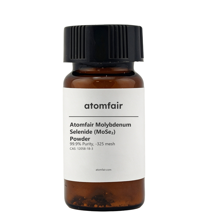
Atomfair Molybdenum Selenide (MoSe2) Powder, 99.9% Purity, -325 mesh
Product Description
Atomfair Molybdenum Selenide (MoSe2) Powder is supplied as a powder with 99.9% purity and -325 mesh. It is intended for transistor, photodetector, photovoltaic, solid-lubricant and energy-storage research.
Technical Specifications |
||||||||||||||||||||||||||
|
Customization & Ordering
Package availability, minimum order quantity, pricing, and lead time are confirmed during quotation.
Key Features and Advantages
- Layered molybdenum selenide with a structure similar to MoS2.
- Indirect bulk band gap of about 0.85 eV and direct monolayer band gap of about 1.5 eV.
- Layered structure supports solid-lubricant, transistor, photodetector and energy-storage research.
APPLICATION SCOPE: transistor, photodetector, photovoltaic, solid-lubricant and energy-storage research
DOCUMENTATION: COA and SDS can be provided upon request for batch-specific confirmation.
LABORATORY PROCUREMENT SUPPORT
For grade selection, particle-size confirmation, documentation support or custom specification review, contact our technical sales team.
What is the difference between the indirect bulk band gap and the direct monolayer band gap of Atomfair MoSe2 powder, and why does this matter for optoelectronic research?
Atomfair MoSe2 powder has an indirect band gap of approximately 0.85 eV in its bulk form and a direct band gap of approximately 1.5 eV in monolayer form. This layer-dependent band structure is critical for designing transistors, photodetectors, and photovoltaic devices, as the direct gap in monolayers enables efficient light absorption and emission.
How does the -325 mesh particle size of this MoSe2 powder benefit solid-lubricant and thin-film deposition research?
The -325 mesh specification ensures a fine powder with particle sizes below approximately 44 microns, which facilitates uniform dispersion in lubricant matrices and consistent thin-film deposition. This physical form is directly intended for solid-lubricant, transistor, photodetector, and energy-storage applications where homogeneous layer formation is essential.
Can a Certificate of Analysis (COA) or Safety Data Sheet (SDS) be provided for batch-specific confirmation of Atomfair MoSe2 powder?
Yes, a Certificate of Analysis (COA) and Safety Data Sheet (SDS) can be provided upon request for batch-specific confirmation, as stated in the product description. These documents support quality verification and safe handling for research and procurement workflows.
Atomfair MoSe₂ powder (99.9%, -325 mesh) offers a layered structure with a thickness-dependent band gap (0.85 eV indirect bulk, 1.5 eV direct monolayer), suitable for transistor, photodetector, photovoltaic, solid-lubricant, and energy-storage research, though exfoliation and particle size considerations apply.
Positive
- High purity 99.9%: The 99.9% purity specification minimizes contamination and batch-to-batch variability, ensuring reproducible results in transistor, photodetector, and photovoltaic research.
- Dual band gap versatility: The indirect bulk band gap of ~0.85 eV and direct monolayer band gap of ~1.5 eV enable both bulk and exfoliated monolayer device studies for optoelectronic and semiconductor applications.
Trade-offs
- Thickness-dependent band gap: The direct band gap is only accessible in monolayer form, requiring mechanical or liquid-phase exfoliation to achieve the desired optoelectronic properties for device fabrication.
- Particle size limitation: The -325 mesh specification (particles <44 µm) may necessitate additional grinding or sieving for thin-film deposition or uniform dispersion in solid-lubricant formulations.
Every advanced material, component, equipment, and instrument in our catalog is backed by rigorous testing. We maintain strict internal quality management frameworks and align with CE conformity metrics to deliver transparent, reproducible performance data via our public open-science repository.
To request raw batch performance data, submit formal vendor registration paperwork, or execute a fast-turnaround R&D manufacturing loop, contact us at inquiry@atomfair.com.
Item is dispatched under the Atomfair Shipping & Delivery Framework (Free worldwide shipping on orders over $59 USD excl. heavy equipment). Return is governed by the Atomfair Return & Refund Policy (7-day technical return window).