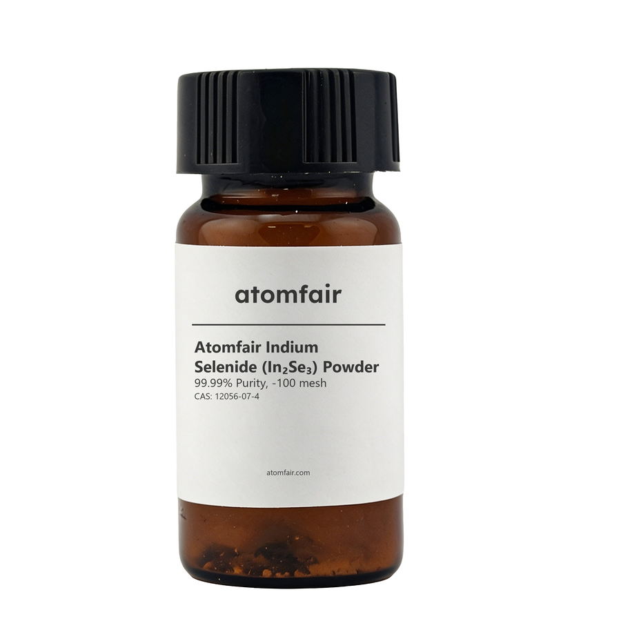
Atomfair Indium Selenide (In2Se3) Powder, 99.99% Purity, -100 mesh
Product Description
Atomfair Indium Selenide (In2Se3) Powder is supplied as a powder with 99.99% purity and -100 mesh. It is intended for photovoltaic, photoelectric-conversion and electronic-device research.
Technical Specifications |
||||||||||||||||||||||||
|
Customization & Ordering
Package availability, minimum order quantity, pricing, and lead time are confirmed during quotation.
Key Features and Advantages
- In2Se3 is an n-type semiconductor compound.
- Black crystalline solid with a density of 5.80 g/cm³.
- Material system is used in photovoltaic, photoelectric-conversion and electronic-device research.
APPLICATION SCOPE: photovoltaic, photoelectric-conversion and electronic-device research
DOCUMENTATION: COA and SDS can be provided upon request for batch-specific confirmation.
LABORATORY PROCUREMENT SUPPORT
For grade selection, particle-size confirmation, documentation support or custom specification review, contact our technical sales team.
What is the significance of 99.99% purity and -100 mesh particle size for Indium Selenide (In2Se3) powder in photovoltaic research?
The 99.99% purity minimizes impurity-induced defects in thin-film devices, which is critical for achieving high efficiency in photovoltaic and photoelectric-conversion research. The -100 mesh specification ensures a consistent powder morphology suitable for uniform deposition during thermal evaporation or sputtering processes, directly supporting reproducible device fabrication as intended for electronic-device research.
Is Indium Selenide (In2Se3) powder suitable as an n-type layer in photovoltaic heterojunctions?
Yes, In2Se3 is specified as an n-type semiconductor compound with a density of 5.80 g/cm³ and is explicitly intended for photovoltaic, photoelectric-conversion, and electronic-device research. Its n-type conductivity makes it a candidate for the n-type layer in heterojunction solar cells or photodetectors, though final device compatibility should be confirmed through experimental evaluation.
What safety and handling documentation is available for Atomfair Indium Selenide (In2Se3) powder?
A Certificate of Analysis (COA) and Safety Data Sheet (SDS) can be provided upon request for batch-specific confirmation. The SDS contains detailed handling, storage, and safety information for the powder, which is a black crystalline solid with CAS number 12056-07-4. Standard laboratory precautions for chalcogenide compounds, including fume hood use and inert atmosphere storage, are recommended per the SDS guidelines.
Atomfair Indium Selenide (In₂Se₃) Powder at 99.99% purity and -100 mesh is a high-purity n-type semiconductor powder suitable for photovoltaic and electronic device research, though the -100 mesh particle size may require additional milling for submicron applications.
Positive
- 99.99% Purity: High purity minimizes contamination in sensitive electronic and photovoltaic device research, ensuring reliable experimental outcomes.
- n-Type Semiconductor: Predetermined n-type conductivity simplifies material selection for device architectures requiring electron-transport layers.
Trade-offs
- -100 Mesh Particle Size: Maximum particle size of 149 µm may be too large for thin-film deposition or solution-processed layers without additional milling.
Every advanced material, component, equipment, and instrument in our catalog is backed by rigorous testing. We maintain strict internal quality management frameworks and align with CE conformity metrics to deliver transparent, reproducible performance data via our public open-science repository.
To request raw batch performance data, submit formal vendor registration paperwork, or execute a fast-turnaround R&D manufacturing loop, contact us at inquiry@atomfair.com.
Item is dispatched under the Atomfair Shipping & Delivery Framework (Free worldwide shipping on orders over $59 USD excl. heavy equipment). Return is governed by the Atomfair Return & Refund Policy (7-day technical return window).