|
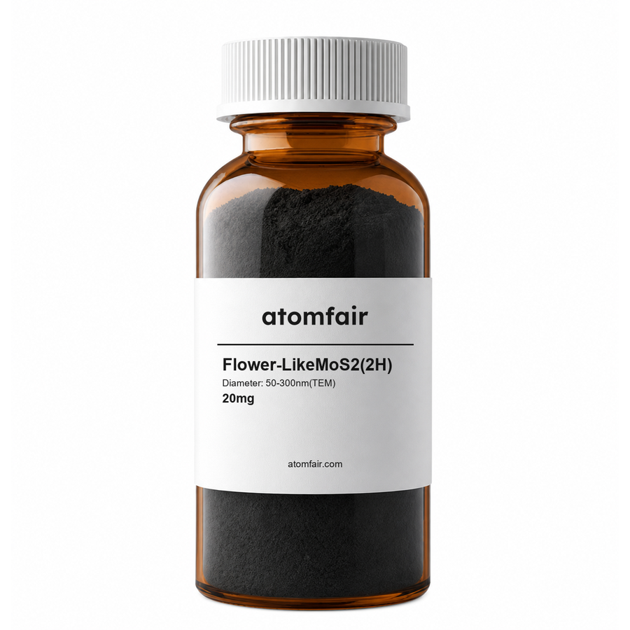
Flower-LikeMoS2(2H), 50-300nm(TEM), 20mg
Product Type: 2D material powder
Research-grade laboratory product
|
|||||||||||||||||||
|
|||||||||||||||||||
|
LABORATORY PROCUREMENT SUPPORT
For material selection, specification confirmation and quotation preparation, contact our technical sales team.
E-MAIL: inquiry@atomfair.com
|
|||||||||||||||||||
|
Manufacturer: Atomfair LLC
Brand: ATOMFAIR®
|
What is the crystal phase of the Flower-Like MoS2 powder and why is it important for semiconductor applications?
The powder is specified as the 2H phase, which is the semiconducting polymorph of MoS2. This phase is stable and widely used in electronic and optoelectronic devices due to its direct bandgap in monolayer form. The flower-like morphology provides high surface area while preserving the 2H crystal structure.
What is the particle size range of this MoS2 powder and how is it measured?
The lateral diameter is 50–300 nm as determined by transmission electron microscopy (TEM). This size range is suitable for solution processing and thin-film fabrication, and the TEM measurement ensures accurate dimensional characterization of the flower-like nanostructures.
Flower-Like MoS2(2H) powder with a diameter of 50-300 nm (TEM) and 20 mg package size offers a high-surface-area morphology for catalytic and electronic applications, but the limited quantity and broad size distribution require careful experimental planning.
Positive
- Flower-like morphology for high surface area: The flower-like structure of MoS2(2H) provides a high surface area beneficial for catalytic and energy storage applications, as indicated by the product name.
- Semiconducting 2H phase: The 2H phase of MoS2 is semiconducting, making it suitable for electronic and optoelectronic devices, as explicitly stated in the product name.
Trade-offs
- Limited quantity of 20 mg: The supplied package size of 20 mg may be insufficient for large-scale experiments or multiple test runs, requiring careful planning and budgeting of material usage.
- Broad particle size distribution: The diameter range of 50-300 nm (TEM) indicates a broad size distribution, which may lead to variability in experimental results and necessitate additional characterization or size-selection steps.
Every advanced material, component, equipment, and instrument in our catalog is backed by rigorous testing. We maintain strict internal quality management frameworks and align with CE conformity metrics to deliver transparent, reproducible performance data via our public open-science repository.
To request raw batch performance data, submit formal vendor registration paperwork, or execute a fast-turnaround R&D manufacturing loop, contact us at inquiry@atomfair.com.
Item is dispatched under the Atomfair Shipping & Delivery Framework (Free worldwide shipping on orders over $59 USD excl. heavy equipment). Return is governed by the Atomfair Return & Refund Policy (7-day technical return window).