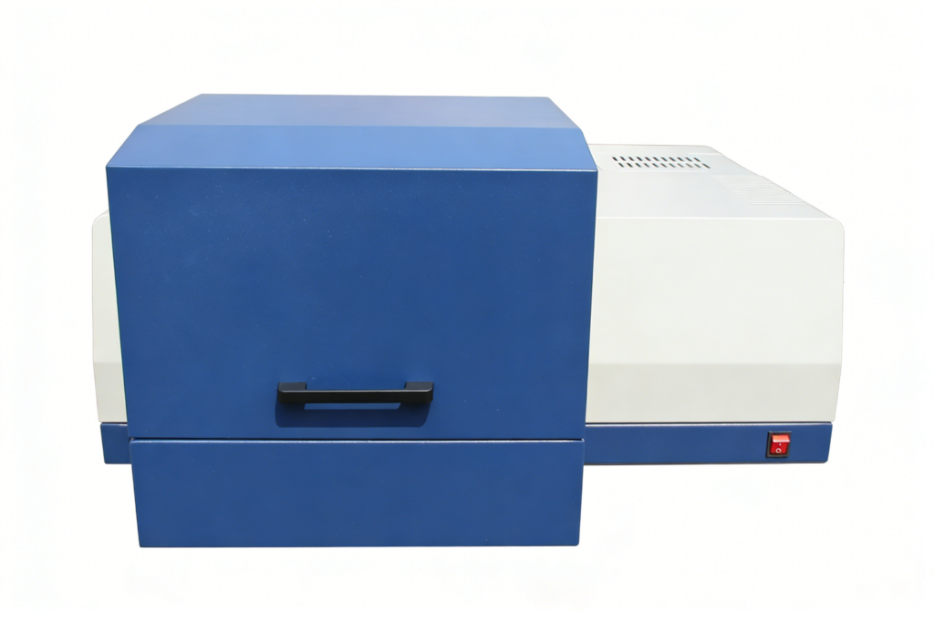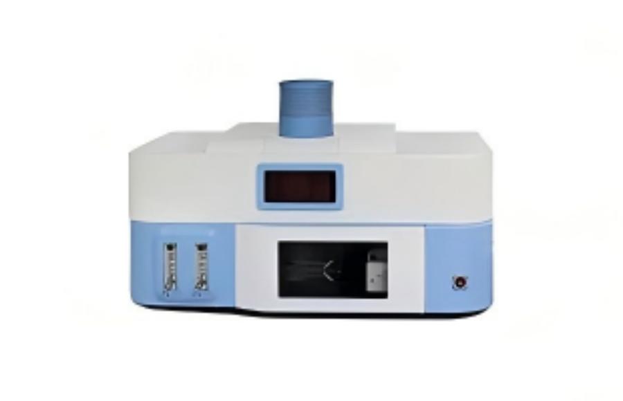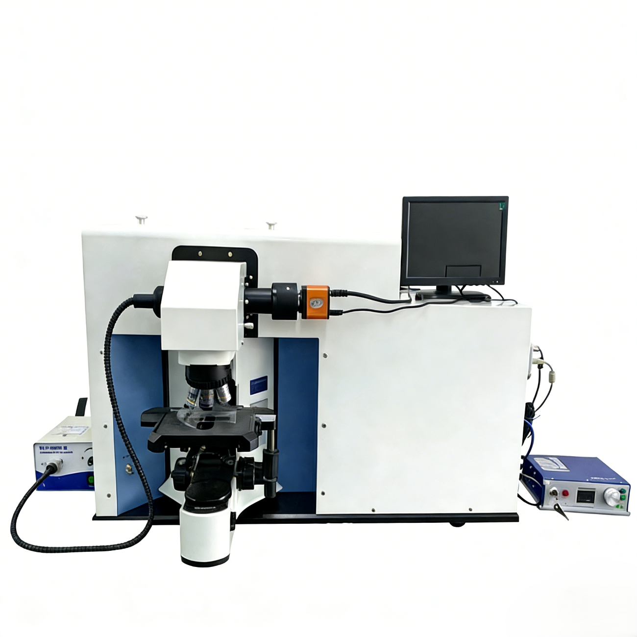
Atomfair-MRS632 Confocal Micro-Raman Spectrometer
Product Overview
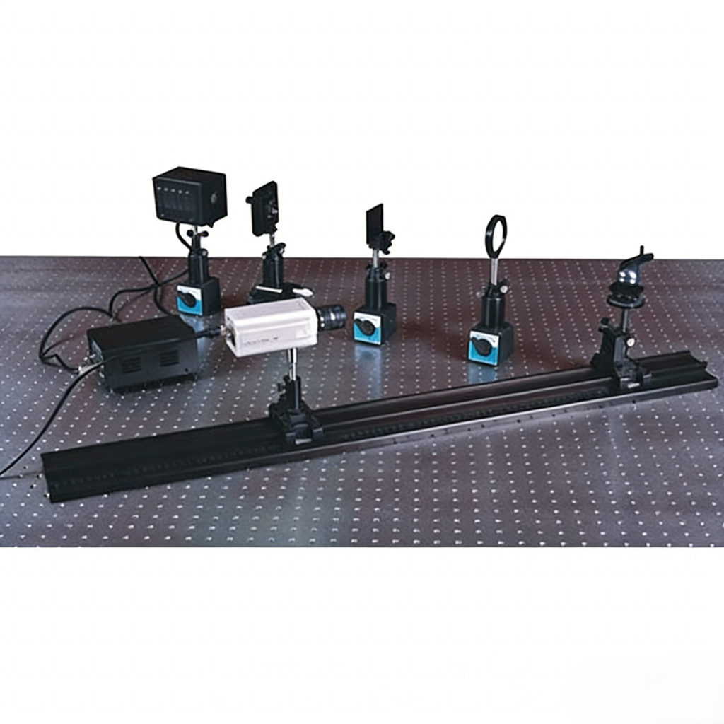
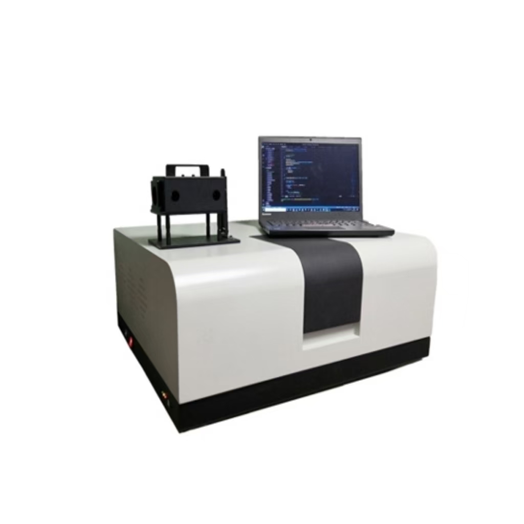
The Atomfair-MRS632 is a research-grade Raman testing instrument equipped with a 3D automatic platform. Adopting a true confocal micro-optical path design, it can quickly and accurately obtain high-resolution spectral images. The instrument features an optimized optical path structure, achieving diffraction-limited spatial resolution while ensuring high light throughput and excellent sensitivity. Combined with an independently developed dedicated operating system, it offers a convenient, efficient, and user-friendly operation process, making it suitable for scientific research and testing scenarios across multiple fields.
Core Product Features
True Confocal Imaging Function: Boasting high spatial resolution, paired with a 3D automatic platform, it enables point-by-point scanning of samples in point, line, surface, and depth directions, clearly presenting the spatial distribution characteristics of the sample’s chemical structure, composition, and physical conditions.
Outstanding Performance: All optical components are optimized, ensuring both spatial and spectral resolution reach the diffraction limit. The high spectral resolution can accurately capture detailed sample information, such as crystallinity integrity, polycrystalline and amorphous identification, stress effects, size effects, etc., simplifying the analysis process.
Ultra-High Sensitivity: Capable of stably observing the fourth-order peak of silicon, it can accurately detect low-content components and weak spectral signals.
Excellent Low-Wavenumber Performance: Covers low-wavenumber spectral ranges that are difficult for ordinary spectrometers to detect, unlocking more sample characteristic information and expanding detection dimensions.
High-Sensitivity Detection System: Equipped with a low-noise, high-sensitivity receiver, it can obtain ideal experimental results in a short time, improving detection efficiency.
Intelligent Variable Pinhole: Software-controlled automatic adjustment of the confocal pinhole eliminates the need for manual operation, adapting to different detection requirements and ensuring detection flexibility and accuracy.
Powerful Software Support: Specifically designed for Raman spectral analysis, it not only supports conventional spectral collection, processing, and analysis but also features Mapping fast automatic scanning function. An optional professional Raman database is available for rapid sample identification and in-depth analysis.
Flexible Configuration Options: Adopting a modular design, it allows customers to select different components and models based on actual needs, meeting personalized requirements while achieving high cost-effectiveness. Multiple lasers and gratings are optional to adapt to various sample tests and experimental result optimization.
Function Expansion Capability: Supports the combination of Raman and Atomic Force Microscopy (AFM), and can be expanded with Tip-Enhanced Raman Spectroscopy (TERS) function, further improving detection accuracy and application scope.
Key Technical Specifications (International Standards)
| Parameter Name | Specifications |
| Measurement Mode | Qualitative/Semi-quantitative Detection |
| Laser (Excitation Wavelength) | 532nm (633nm, 785nm Expandable) |
| Spectral Range | 50~7000cm⁻¹ |
| Spectral Resolution | ≤1cm⁻¹ |
| Wavelength Accuracy | ≤±1cm⁻¹ |
| Sensitivity | Observable Fourth-Order Peak of Silicon |
| Spatial Resolution | x/y Axis: 0.01μm; z Axis: 0.002μm (Related to the Fine-Tuning Gear Reduction Ratio of the Microscope) |
| Mapping Stroke | 3 Inches × 2 Inches |
| CCD Spectral Detector Size | 26.6×3.2mm |
| Effective Pixels | 1650×200 |
| Pixel Size | 16×16μm |
| Confocal Pinhole | 50μm, 150μm, 200μm, 400μm |
Applicable Sample Types
Surface-Enhanced Raman Spectroscopy (SERS)-Related Samples: Such as Rhodamine 6G (also known as Rose Bengal 6G, Rhodamine 590, Basic Yellowish Red), with the molecular formula C₂₈H₃₁N₂O₃Cl. It appears as a red or yellowish-brown powder, soluble in water to form a scarlet solution with green fluorescence, and soluble in alcohol to form a red solution with yellow fluorescence or a yellowish-red solution with green fluorescence. It is highly hazardous to humans and other organisms.
Superconducting Materials: Such as Yttrium Barium Copper Oxide (YBCO), the first material with a superconducting temperature above 77K. Its superconducting transition temperature is higher than the boiling point of liquid nitrogen (77K), and it can be cooled with relatively inexpensive liquid nitrogen (traditional superconductors require cooling with liquid helium at 4.2K or liquid hydrogen at 20K). It is suitable for use as magnets in nuclear magnetic resonance imaging, maglev facilities, and Josephson junctions. Its structure is a perovskite defect-type layered structure, containing alternating CuO-CuO₂-CuO₂-CuO layers. The CuO₂ layers can be deformed and wrinkled, yttrium atoms are present between the CuO₂ layers, and the BaO layer is located between the CuO and CuO₂ layers.
Semiconductor Materials:
Gallium Nitride (GaN): A compound of nitrogen and gallium, it is a direct bandgap semiconductor with a wurtzite-like structure and high hardness. With an energy gap width of 3.4 electron volts, it is suitable for high-power, high-speed optoelectronic components and has been widely used in light-emitting diodes since 1990.
Gallium Arsenide (GaAs): A compound of gallium and arsenic, it is a III-V direct bandgap semiconductor with a zinc blende crystal structure. It is used in the manufacture of microwave frequency integrated circuits, monolithic microwave integrated circuits, infrared light-emitting diodes, laser diodes, solar cells, optical windows, and other devices. GaAs is often used as a substrate material for the epitaxial growth of other III-V semiconductors, including indium gallium arsenide and aluminum gallium arsenide.
Polymer Materials:
Polystyrene (PS): An amorphous polymer, the side groups of its macromolecular chains are benzene rings, and the random arrangement of these large-volume side groups determines the physical and chemical properties of polystyrene. The symmetric breathing vibration of cyclic compounds is often the strongest Raman band. Therefore, the main characteristic peaks of the Raman spectrum of polystyrene (PS) are 618cm⁻¹, 1000cm⁻¹ (ring breathing), 1029cm⁻¹, 1199cm⁻¹, 1601cm⁻¹ (C=C benzene ring), etc.
Nylon (PA): The infrared spectra of different types of nylon are very similar, but the backbones composed of different methylene sequences show strong bands in the Raman spectrum, enabling rapid differentiation.
Advantages of Raman Spectroscopy (Compared with Infrared Spectroscopy)
Complementary Information: Due to differences in spectral principles, the information provided by the two spectra varies. Groups with high symmetry and low polarity (such as C-C, C=C, S-S) have weak infrared absorption but strong bands in Raman spectra, making them suitable for Raman detection. Infrared spectroscopy is mostly used to determine the side groups and end groups of polymers, while Raman spectroscopy is more suitable for studying the backbone structure of polymers, forming a complementary relationship.
Convenient Sample Preparation: In most cases, samples do not require pretreatment and can be directly tested in any form of polymer material, even in transparent containers, which is particularly convenient for the detection of liquid samples.
Suitable for Aqueous Solution Research: Water has extremely strong infrared absorption, while its Raman scattering is weak, with only a weak spectral peak near 1640cm⁻¹. Therefore, Raman spectroscopy is particularly suitable for the study of aqueous solution systems.
Typical Cooperation Users
Hubei Minzu University, Shangrao Normal University, Guizhou University, Guangxi Normal University for Nationalities, Hebei Laser Research Institute, Shandong University Weihai Industry Research Institute, Northeast Institute of Geography and Agroecology, Chinese Academy of Sciences, Hangzhou Liangzhu Ancient City Ruins World Heritage Monitoring and Management Center, etc.
If you’re interested, have any questions, or have specific customization requirements, please feel free to contact us at inquiry@atomfair.com.
How does the Atomfair-MRS632's true confocal design with software-controlled pinhole (50–400 µm) impact the trade-off between spatial resolution and signal intensity for depth profiling of layered materials?
The confocal pinhole size directly controls depth discrimination and lateral resolution: smaller pinholes (e.g., 50 µm) maximize spatial resolution (x/y step 0.01 µm, z step 0.002 µm) but reduce signal throughput, while larger pinholes (400 µm) increase signal but degrade depth resolution. The MRS632's optimized optics and high-sensitivity CCD (1650×200 pixels, 16×16 µm pixel size) partially compensate for this trade-off, enabling detection of weak signals such as the fourth-order peak of silicon even at moderate pinhole settings. The instrument's true confocal path ensures that only light from the focal plane reaches the detector, making it suitable for depth-resolved analysis of layered structures.
What excitation laser wavelengths can be used with the Atomfair-MRS632, and which applications benefit most from each wavelength given the spectral range of 50–7000 cm⁻¹?
The MRS632 comes standard with a 532 nm laser and supports expansion to 633 nm and 785 nm. The 532 nm excitation provides high Raman scattering intensity, ideal for sensitive measurements on inorganic materials like semiconductors (GaN, GaAs) and superconductors (YBCO), but may induce fluorescence in organic or biological samples. The 633 nm laser reduces fluorescence and is preferred for polymer characterization (e.g., polystyrene, nylon) and SERS studies. The 785 nm laser further minimizes fluorescence, making it optimal for colored, fluorescent, or biological samples. With a spectral range of 50–7000 cm⁻¹, the instrument captures both low-wavenumber lattice modes and high-wavenumber molecular vibrations across all laser lines.
What are the sample size and mounting constraints for the MRS632's 3D automatic mapping stage, and how does the motorized stage affect high-resolution imaging throughput?
The mapping stage has a stroke of 3 inches × 2 inches (approx. 76 mm × 51 mm), limiting the maximum scan area. Samples must fit within these dimensions and be compatible with the confocal geometry (flat, reflective, and able to be positioned under the objective). The 3D automatic platform enables point, line, surface, and depth scanning with x/y steps as fine as 0.01 µm and z steps of 0.002 µm. While this allows diffraction-limited spatial resolution, mapping a large area at high resolution can be time-consuming due to the point-by-point acquisition. The true confocal design ensures that only light from the focal plane is collected, improving depth resolution for thick or structured samples but also requiring precise sample flatness and focus stability throughout the scan.
The Atomfair-MRS632 Confocal Micro-Raman Spectrometer delivers diffraction-limited spatial and spectral resolution with true confocal imaging, enabling high-sensitivity detection down to the fourth-order silicon peak and low-wavenumber coverage to 50 cm⁻¹, while its modular design supports flexible configuration for diverse research applications.
Positive
- True confocal imaging with 3D mapping: The true confocal optical path with a 3D automatic platform enables point-by-point scanning in point, line, surface, and depth directions, providing high spatial resolution (x/y: 0.01 μm, z: 0.002 μm) to reveal chemical and structural distribution.
- Ultra-high sensitivity and low-wavenumber coverage: Stable observation of the fourth-order silicon peak confirms ultra-high sensitivity for trace analysis, while the 50 cm⁻¹ low-wavenumber limit accesses spectral features invisible to standard spectrometers, expanding detection capabilities.
Trade-offs
- Requires careful sample and environment handling: The instrument's sensitivity to low-content components and weak signals demands precise sample preparation and stable environmental conditions to avoid artifacts, especially for SERS samples like Rhodamine 6G, which are hazardous and require proper safety protocols.
- Spatial resolution depends on microscope gear ratio: The stated spatial resolution (x/y: 0.01 μm; z: 0.002 μm) is related to the fine-tuning gear reduction ratio of the microscope, meaning actual performance may vary with the specific configuration selected, requiring careful setup to achieve optimal results.
Every advanced material, component, equipment, and instrument in our catalog is backed by rigorous testing. We maintain strict internal quality management frameworks and align with CE conformity metrics to deliver transparent, reproducible performance data via our public open-science repository.
To request raw batch performance data, submit formal vendor registration paperwork, or execute a fast-turnaround R&D manufacturing loop, contact us at inquiry@atomfair.com.
Item is dispatched under the Atomfair Shipping & Delivery Framework (Free worldwide shipping on orders over $59 USD excl. heavy equipment). Return is governed by the Atomfair Return & Refund Policy (7-day technical return window).