
Advanced Engineered & Heterogeneous Substrates
Advanced Engineered & Heterogeneous Substrates are designed for semiconductor, electronics, optoelectronics, power-device, MEMS, sensor, and research applications that require specialized performance, composite structures, or customized surfaces. These substrates are engineered around requirements such as electrical insulation, thermal conductivity, high-temperature stability, mechanical strength, lattice matching, optical transmission, chemical resistance, and downstream processing compatibility.
This category includes ceramic substrates, engineered single-crystal substrates, glass and quartz substrates, composite and metallized substrates, as well as bonded, coated, and heterogeneous structures. Products may be supplied as plates, wafers, square substrates, round substrates, thin-film carrier substrates, or custom-machined components. Because material and structural properties vary significantly, selection should begin with the intended application, followed by material system, dimensions, thickness, surface condition, and structural design.
Show More: Engineered and Heterogeneous Substrates
Choose by Material and Structure
| Product Type | Typical Materials | Performance Priorities | Common Forms |
|---|---|---|---|
| Alumina ceramic substrates | 96% Al2O3, high-purity alumina | Electrical insulation, dimensional stability, heat resistance, general-purpose use | Square plates, thin sheets, thick plates, round substrates, package bases |
| Silicon nitride ceramic substrates | Si3N4 | High mechanical strength, thermal-shock resistance, balanced insulation and heat transfer | Thin substrates, square plates, thick plates, structural supports |
| Zirconia ceramic substrates | ZrO2 | Toughness, wear resistance, high-temperature capability, insulating support | White or black ceramic plates, square substrates, custom parts |
| Aluminum nitride ceramic substrates | AlN | High thermal conductivity combined with electrical insulation | Power-module substrates, thin sheets, metallized substrates |
| Silicon carbide substrates | SiC | High-temperature, high-power, and chemical-resistance requirements | Single-crystal wafers, polished wafers, epitaxial carrier substrates |
| Sapphire substrates | Single-crystal Al2O3 | Optical transmission, hardness, high-temperature stability, insulation | Round wafers, square plates, polished substrates, optoelectronic substrates |
| Quartz and fused-silica substrates | SiO2 | Low thermal expansion, optical performance, cleanliness, chemical resistance | Round wafers, square plates, optical windows, laboratory substrates |
| Glass substrates | Borosilicate, aluminosilicate, low-alkali, and specialty glass | Transparency, flatness, insulation, and visual process access | Square plates, round wafers, thin glass, MEMS substrates |
| Composite and metallized substrates | Ceramic-metal, ceramic-ceramic, coated, and copper-clad structures | Thermal transfer, electrical connection, joining, and package integration | DBC, AMB, copper-clad substrates, coated substrates |
| Heterogeneous and bonded substrates | SOI, SOS, heteroepitaxial carrier substrates, bonded wafers | Combined device and handle layers, isolation, lattice matching, thermal matching | Round wafers, bonded wafers, transferred-film structures |
Select According to Your Application
| If Your Main Requirement Is | Materials to Compare First | Specifications to Confirm |
|---|---|---|
| Electrical insulation and isolation | Alumina, silicon nitride, aluminum nitride, zirconia, glass, sapphire | Breakdown strength, thickness, edge distance, surface cleanliness, working voltage |
| Heat dissipation and power-device packaging | Aluminum nitride, silicon nitride, metallized ceramics, copper-clad ceramics | Thermal conductivity, thermal resistance, metal-layer thickness, joining method, thermal cycling |
| High-temperature or thermal-shock environments | Silicon nitride, aluminum nitride, zirconia, sapphire, quartz, SiC | Operating temperature, heating and cooling rate, atmosphere, load, dimensional change |
| Optical, ultraviolet, or infrared applications | Sapphire, quartz, fused silica, specialty glass | Transmission range, surface quality, flatness, double-side polishing, defect level |
| MEMS, sensors, and microfabrication | Silicon, SOI, glass, quartz, sapphire, ceramics | Wafer size, crystal orientation, insulating or device-layer thickness, bonding, etching compatibility |
| RF, microwave, or high-frequency devices | High-resistivity silicon, sapphire, quartz, ceramic composite substrates | Dielectric constant, loss, surface roughness, frequency range, metallization method |
| Chemical, vacuum, or clean-process environments | Quartz, sapphire, SiC, high-purity ceramics, low-alkali glass | Chemical media, vacuum level, particle control, cleaning method, bake temperature |
| Custom shapes or assembly integration | Engineering ceramics, glass, quartz, metallized composite substrates | Drawing, tolerances, holes, slots, chamfers, edge treatment, quantity, inspection requirements |
How to Read Substrate Specifications
Before selecting a product, define the essential requirements in the following groups:
- Dimensions and geometry: wafer diameter, plate length and width, thickness, dimensional tolerances, roundness, holes, and notches.
- Material and grade: chemical composition, purity, crystal structure, crystal orientation, doping, resistivity, or ceramic grade.
- Surface condition: polished, lapped, sintered, coated, metallized, roughness, flatness, warp, and particle requirements.
- Structural format: single-layer substrate, composite substrate, copper-clad substrate, bonded wafer, insulating-layer structure, or thin-film carrier.
- Thermal and electrical performance: thermal conductivity, coefficient of thermal expansion, dielectric constant, dielectric loss, breakdown strength, and operating-temperature range.
- Processing and delivery: single pieces or multi-piece packs, standard or custom dimensions, chamfering, drilling, cutting, cleaning, and inspection documentation.
Common Application Areas
Engineered substrates are used for electronic packaging and electrical insulation, power modules and thermal-management structures, LED and optoelectronic devices, RF and microwave circuits, MEMS and sensors, thin-film deposition and epitaxial research, vacuum and high-temperature processing, laboratory fixtures, and customized device development. When a project requires several material properties within one structure, composite, coated, metallized, or bonded substrates can help balance insulation, thermal transfer, electrical conduction, optical performance, and mechanical stability.
Custom Substrates and Special Structures
When a standard substrate does not meet the application requirements, custom solutions may be evaluated according to the drawing and process conditions. Options may include non-standard dimensions, shaped cutting, holes and slots, chamfers, double-side polishing, metallization, copper cladding, insulating layers, surface coatings, wafer bonding, and thin-film carrier structures. For an inquiry, provide the material, dimensions, thickness, tolerances, surface requirements, operating temperature, environment, quantity, and downstream process so the appropriate substrate structure can be identified.
Frequently Asked Questions
What is the difference between an engineered substrate and a standard ceramic plate?
Engineered substrates are selected and processed according to requirements such as electrical insulation, heat transfer, thermal expansion, surface finish, cleanliness, or device-processing compatibility. They are not simply general support plates. The exact distinction should be confirmed from the product material, dimensions, surface condition, and performance specifications.
Should I choose alumina, silicon nitride, or aluminum nitride?
For general electrical insulation and dimensional stability, alumina is often a practical starting point. When mechanical strength and thermal-shock resistance are more important, compare silicon nitride. When higher heat dissipation is required while maintaining electrical insulation, aluminum nitride is often considered. Final selection should also account for thickness, joining method, and operating temperature.
Should I choose glass, quartz, or sapphire for a transparent substrate?
Glass is suitable for general transparency, insulation, and flat support. Quartz is preferred for low thermal expansion, chemical resistance, and high-cleanliness environments. Sapphire is suitable when high hardness, high-temperature performance, or a specific optical wavelength range is required. Selection should consider wavelength, temperature, surface quality, and processing method.
Can ceramic substrates be used directly for coating, printing, or metallization?
Suitability depends on surface roughness, flatness, cleanliness, ceramic grade, and the specific process. Before ordering, confirm whether the surface is polished, lapped, or sintered, and specify the intended deposition, printing, soldering, adhesive bonding, or metallization method.
How should I determine the substrate thickness?
Thickness should be selected by considering mechanical support, electrical insulation, thermal resistance, processing strength, and available installation space. Thin substrates are often used for lightweight structures, microfabrication, and thin-film processes, while thicker plates are preferred for support, fixtures, and high-rigidity applications. Voltage, temperature, and mechanical loads should be evaluated as part of the complete structure.
How do I choose between a round wafer and a square substrate?
Round wafers are commonly used for wafer-level processing, spin coating, thin-film deposition, and rotating equipment. Square substrates are often more convenient for cutting, laboratory fixtures, packaging, and custom assembly. Equipment clamping, usable area, and edge-treatment requirements should also be confirmed.
Can drilling, cutting, chamfering, or custom shaping be provided?
Special machining can be evaluated according to the material and technical drawing. Provide the dimensions, tolerances, hole or slot locations, edge treatment, surface requirements, quantity, and operating environment so the machining method and inspection requirements can be reviewed.
What information is needed for an inquiry about a heterogeneous or bonded substrate?
Please specify the material combination, wafer or plate dimensions, crystal orientation, thickness of each layer, insulating or device-layer requirements, surface condition, bonding method, operating temperature, and downstream process. More complete information makes it easier to identify a suitable structure and specification.
Showing 193–207 of 207 results
-
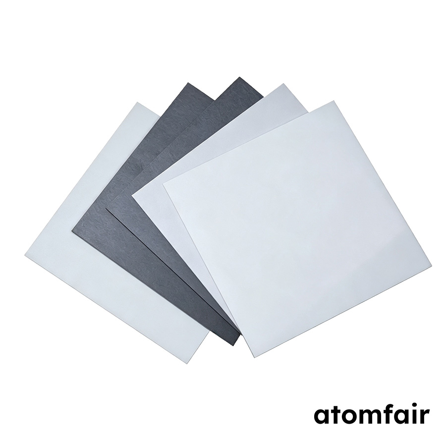
Zirconia Ceramic Plate 150×150×2 mm, 94% ZrO2
$62.00 -
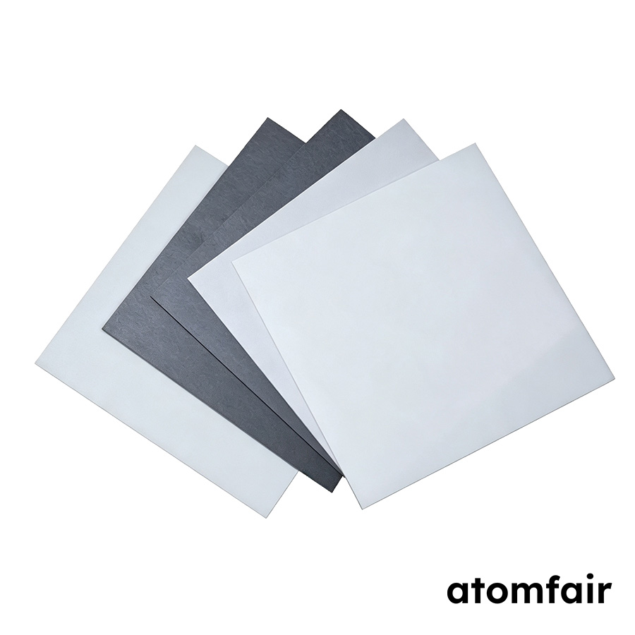
Zirconia Ceramic Plate 20×20×1 mm White Pack of 10
$31.00 -
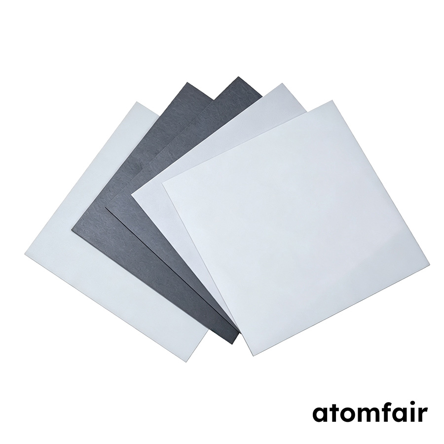
Zirconia Ceramic Plate 50×50×0.5 mm Black
$48.00 -
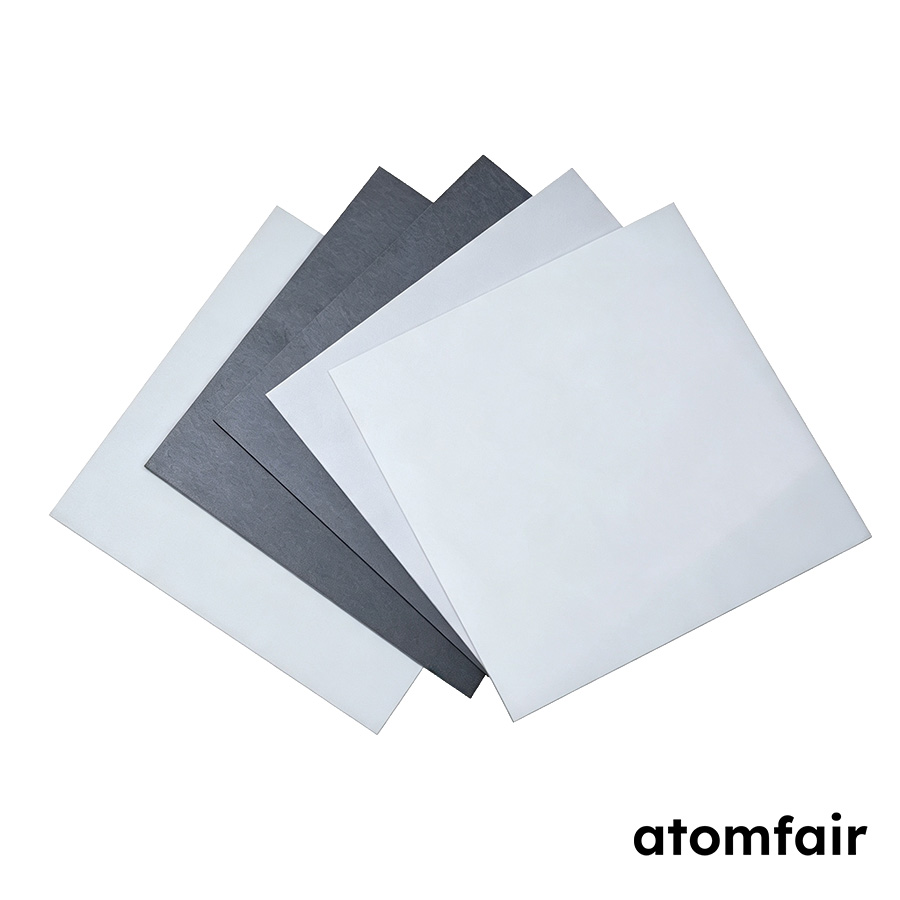
Zirconia Ceramic Plate 50×50×0.5 mm ZrO2 ≥94%
$39.00 -
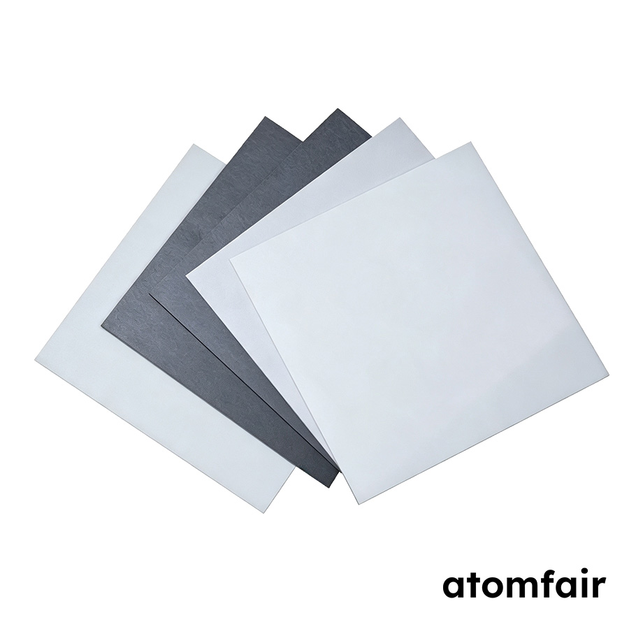
Zirconia Ceramic Plate 50×50×1 mm Black Pack 10
$66.00 -
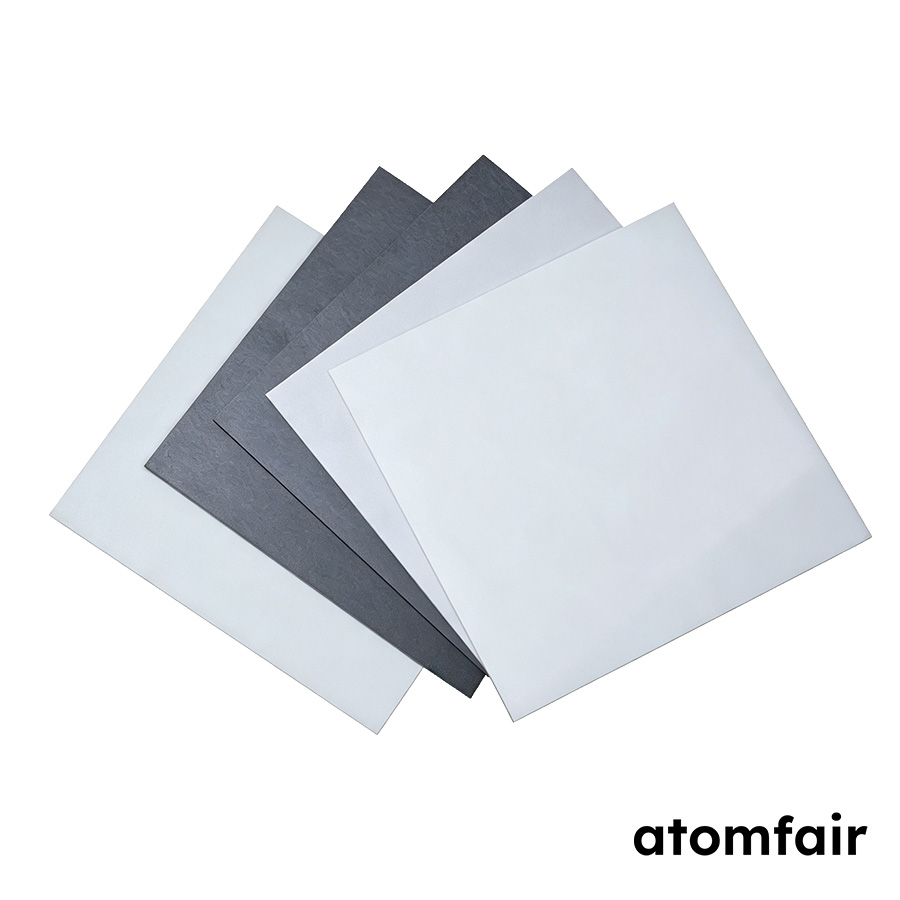
Zirconia Ceramic Plate 50×50×1 mm ZrO2 94%
$44.00 -
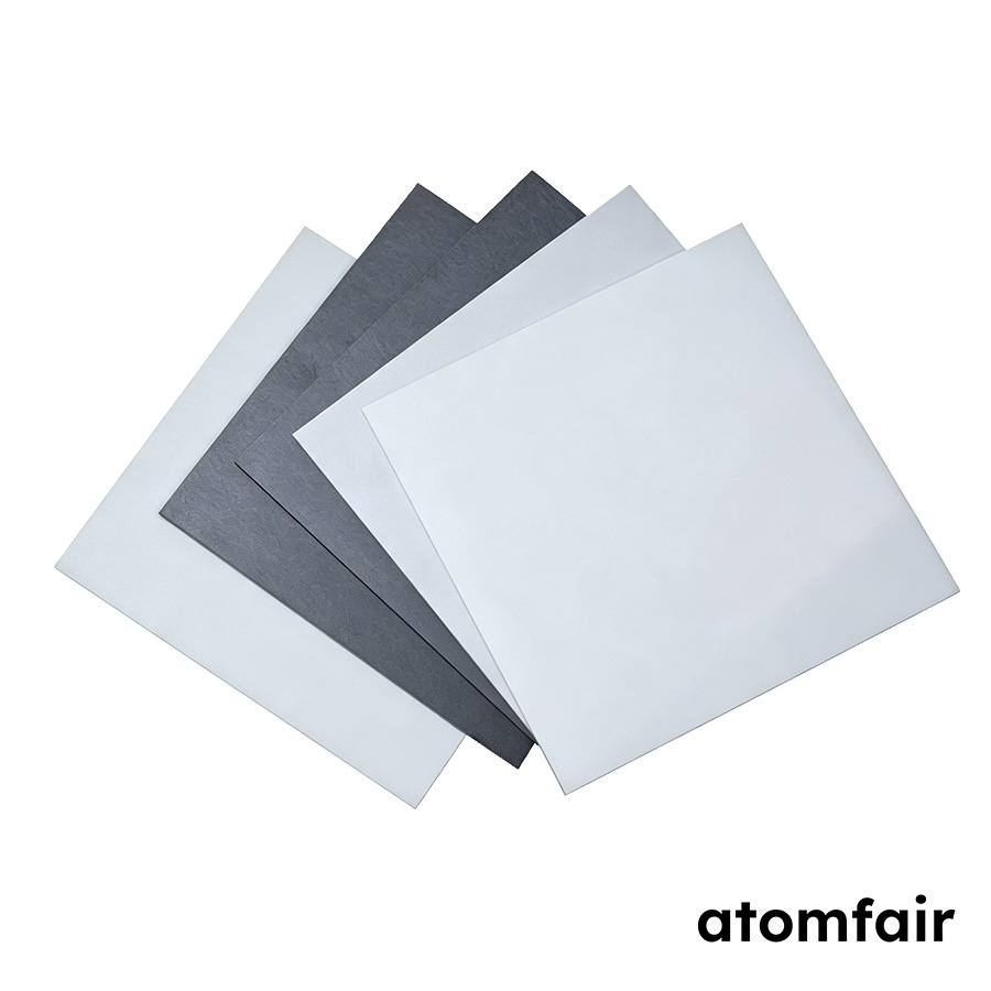
Zirconia Ceramic Plate 50×50×2 mm Black, 10 Pack
$83.00 -
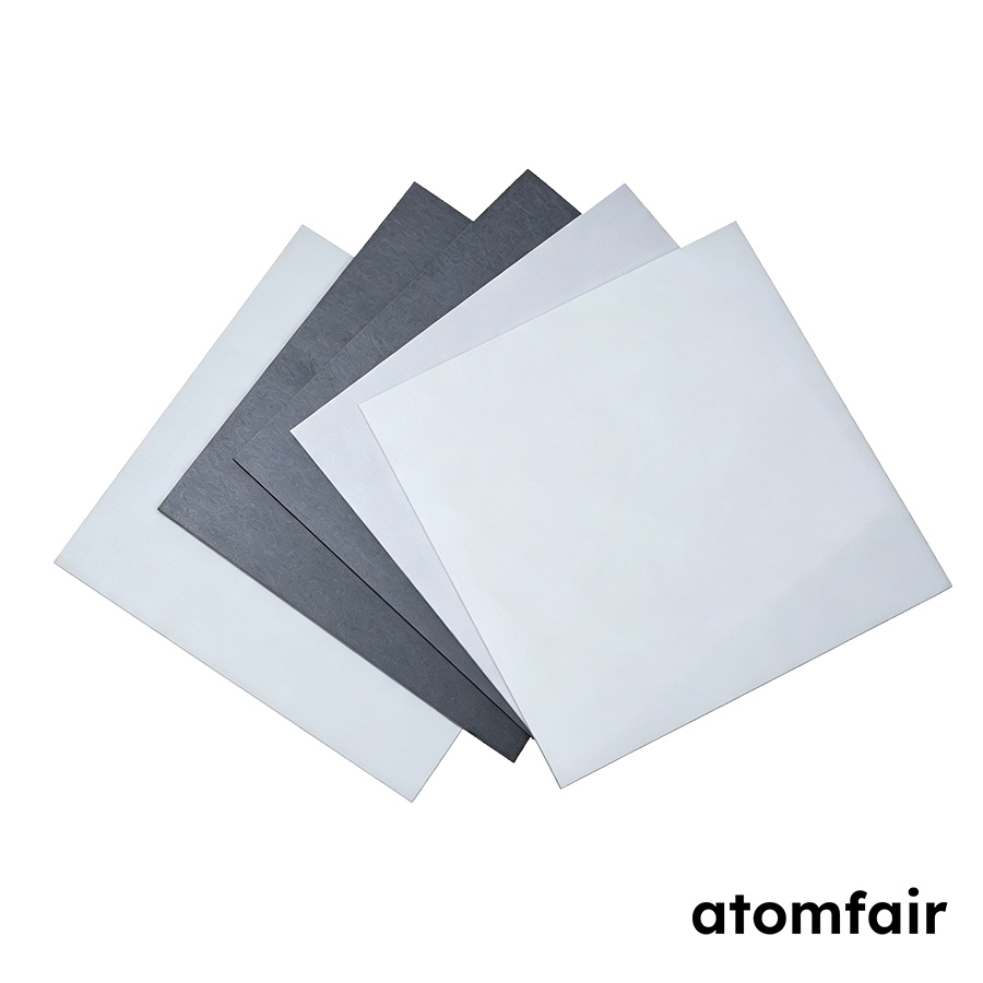
Zirconia Ceramic Plate 50×50×2 mm ZrO2 ≥94%
$66.00 -
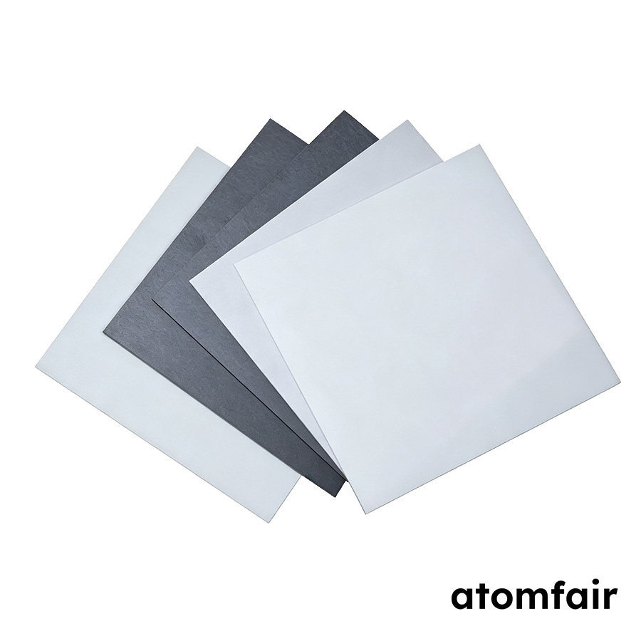
Zirconia Ceramic Plate 50×50×3 mm ZrO2 ≥94%
$101.00 -
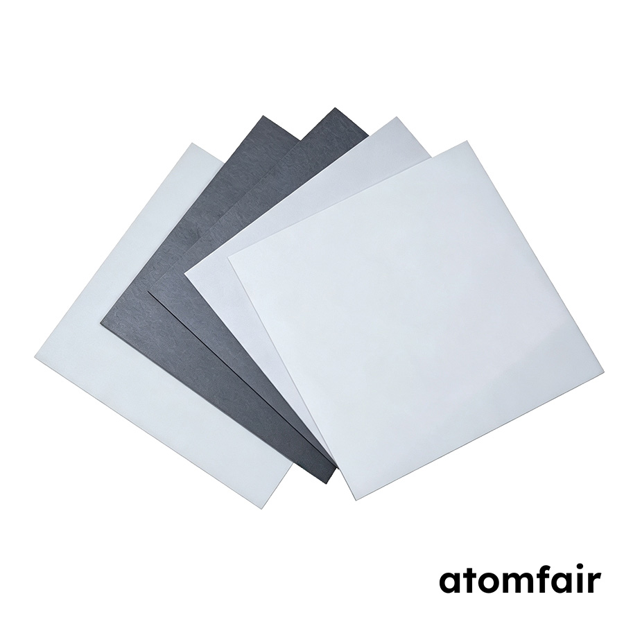
Zirconia Ceramic Plate 50×50×4 mm ZrO2 94%
$119.00 -
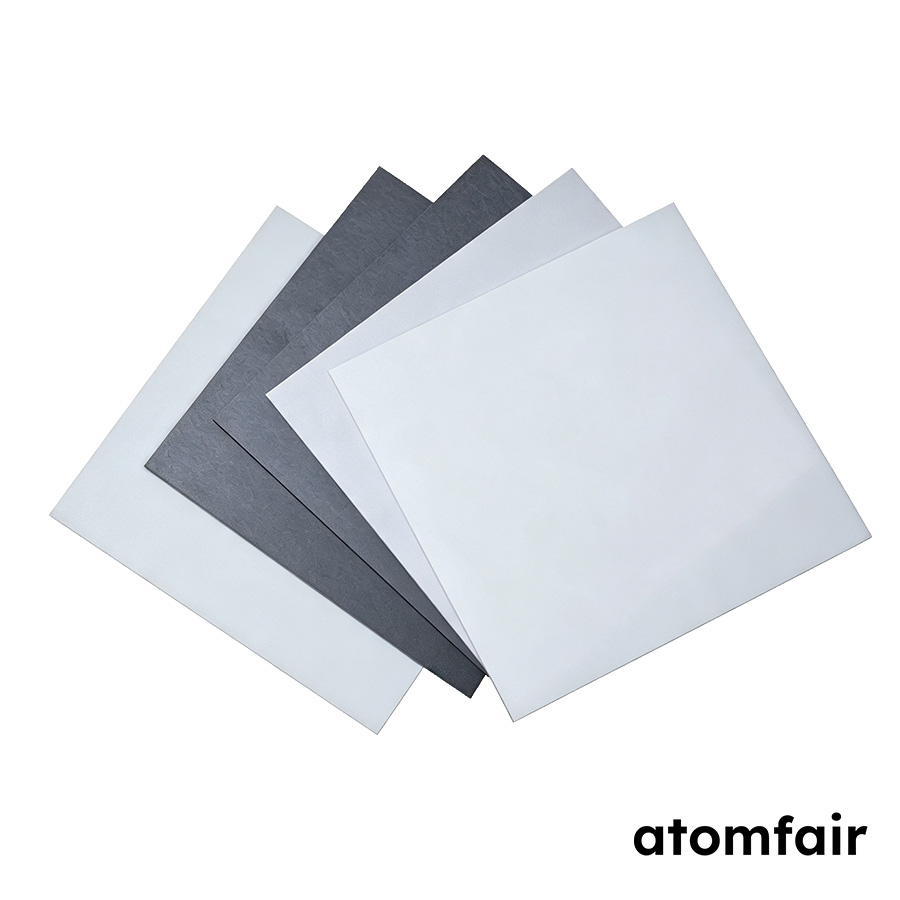
Zirconia Ceramic Plate 50×50×5 mm 94% ZrO2
$136.00 -
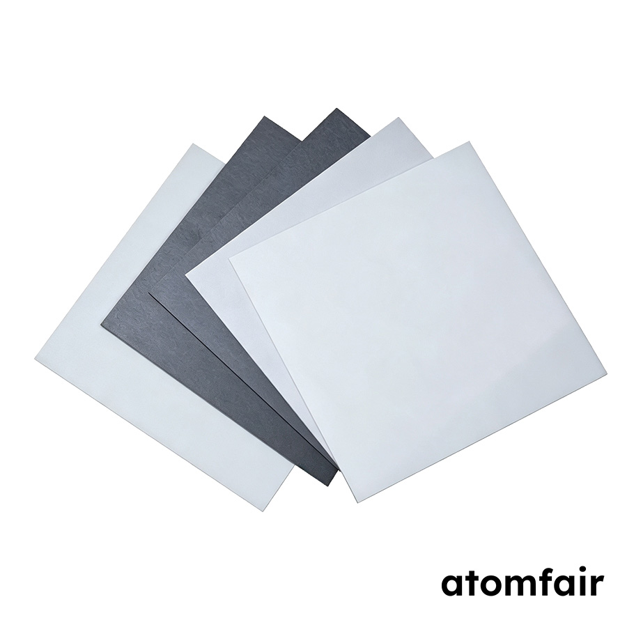
Zirconia Ceramic Plate 94% ZrO2 10×10×1 mm White
$13.00 -
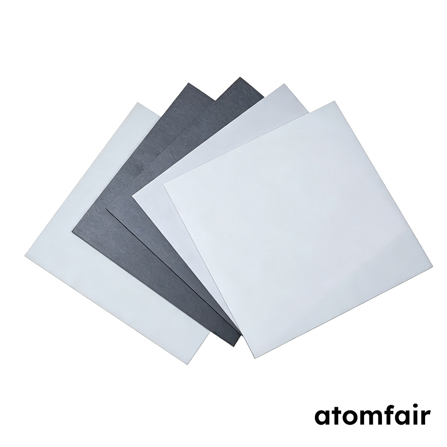
Zirconia Ceramic Plate 94% ZrO2 100×100×2 mm
$225.00 -
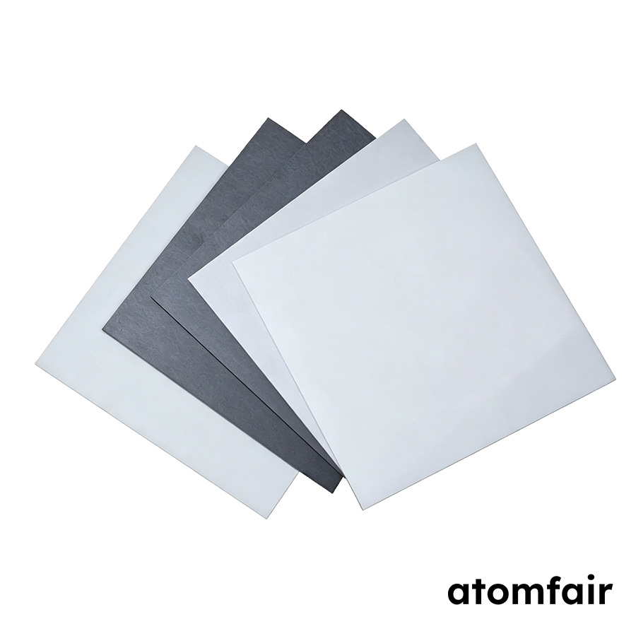
Zirconia Ceramic Plate 94% ZrO2 20×20×2 mm
$48.00 -
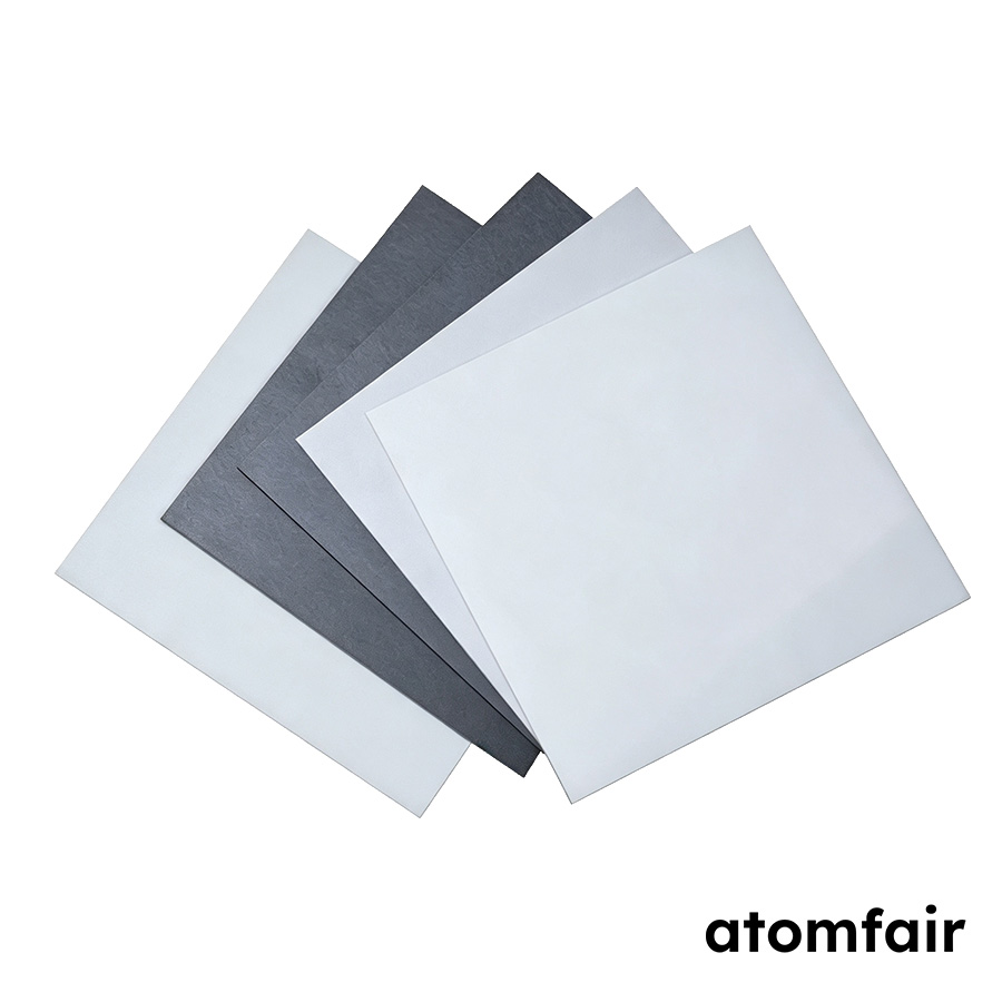
ZrO2 Zirconia Ceramic Plate 10×10×2 mm Black
$31.00