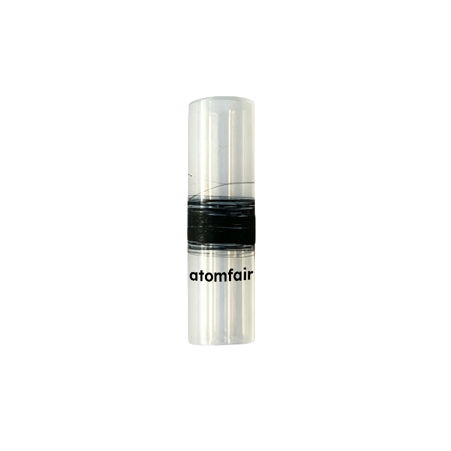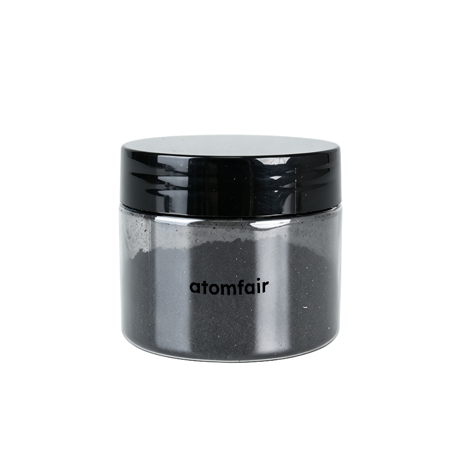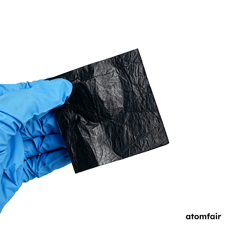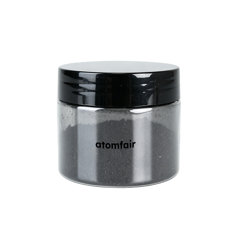
Highlyconductive single-walledcarbon nanotubes, OD 1-2 nm, length 5-30um; Cond>2000 s/cm; SSA>1075 m2/gor; SSA>600 m2/g, purity >95%Product Type: Single-walled carbon nanotube material
Research-grade laboratory product
|
|||||||||||||||||||||
|
|||||||||||||||||||||
|
LABORATORY PROCUREMENT SUPPORT
For model selection, material specification matching, application fit or quotation confirmation, contact our technical sales team.
E-MAIL: inquiry@atomfair.com
|
|||||||||||||||||||||
|
Manufacturer: Atomfair LLC
Brand: ATOMFAIR?
|
What are the key electrical and surface area specifications of the AF-SWCNT-S30 single-walled carbon nanotubes?
The AF-SWCNT-S30 single-walled carbon nanotubes have an outer diameter of 1–2 nm, length 5–30 µm, electrical conductivity >2000 S/cm, specific surface area >1075 m²/g (with an additional SSA >600 m²/g noted), and purity >95%. These specifications make the material suitable for high-performance electrode, composite, and conductive film applications.
In what research applications are the AF-SWCNT-S30 single-walled carbon nanotubes typically used?
The product is designed for dispersion, composite, film, electrode, and conductivity research workflows. It can be matched to applications requiring pristine, hydroxylated, carboxylated, amino-modified, graphitized, doped, or coated grades, depending on the specific experimental or formulation needs.
What information is required to request a quotation for the AF-SWCNT-S30 product?
To request a quotation, include the nanotube wall type, functionalization, diameter/length range, package size, and quantity. The product is available in two specification models (AF-SWCNT-S30-P2000 and AF-SWCNT-S30-P2500), so confirm the desired model. Contact technical sales at inquiry@atomfair.com for further assistance.
This single-walled carbon nanotube material (AF-SWCNT-S30) offers a high electrical conductivity of >2000 S/cm and a large specific surface area (>1075 m²/g), making it suitable for conductive composite, electrode, and nanocarbon research applications, though its nanoscale dimensions and high surface area require careful handling and dispersion.
Positive
- High electrical conductivity: With a conductivity exceeding 2000 S/cm, this material is well-suited for applications requiring efficient charge transport, such as conductive films, electrodes, and composite formulations.
- Large specific surface area: The specific surface area greater than 1075 m²/g provides extensive interfacial contact, which is beneficial for catalysis, adsorption, and electrochemical applications where surface activity is critical.
Trade-offs
- Nanoscale dimensions require careful handling: The outer diameter of 1-2 nm and length of 5-30 µm present inhalation and dispersion challenges; appropriate safety protocols and dispersion techniques are necessary during laboratory handling.
- High surface area may complicate processing: The high specific surface area can lead to agglomeration and increased viscosity in liquid dispersions, requiring optimized sonication or surfactant-based methods to achieve uniform dispersion.
Every advanced material, component, equipment, and instrument in our catalog is backed by rigorous testing. We maintain strict internal quality management frameworks and align with CE conformity metrics to deliver transparent, reproducible performance data via our public open-science repository.
To request raw batch performance data, submit formal vendor registration paperwork, or execute a fast-turnaround R&D manufacturing loop, contact us at inquiry@atomfair.com.
Item is dispatched under the Atomfair Shipping & Delivery Framework (Free worldwide shipping on orders over $59 USD excl. heavy equipment). Return is governed by the Atomfair Return & Refund Policy (7-day technical return window).