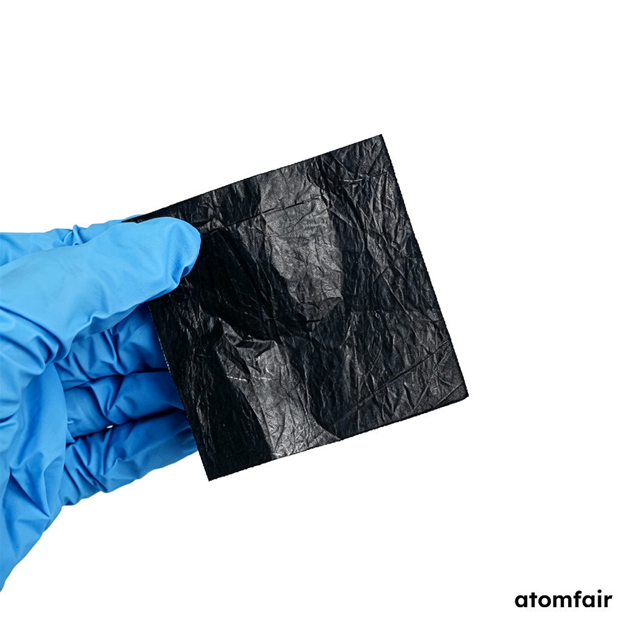
Aligned arrays of multiwalled carbon nanotube silicon oxide substrate, conductivity 10^3 S/m, diameter 3-10 nmProduct Type: Carbon nanotube array material
Research-grade laboratory product
|
|||||||||||||||||||||||
|
|||||||||||||||||||||||
|
LABORATORY PROCUREMENT SUPPORT
For model selection, material specification matching, application fit or quotation confirmation, contact our technical sales team.
E-MAIL: inquiry@atomfair.com
|
|||||||||||||||||||||||
|
Manufacturer: Atomfair LLC
Brand: ATOMFAIR®
|
How does the density constraint (≤0.3 g/cm³) influence the electrical and structural performance of this aligned MWCNT array over the 100–1000 µm height range?
The specified density ≤0.3 g/cm³ for the 100–1000 µm height range indicates a sparse, vertically aligned structure that maximizes accessible surface area for electrolyte infiltration in electrochemical applications. This low density is consistent with the ~20 m²/g specific surface area and supports field-emission and electrode integration workflows by providing direct conduction pathways while maintaining structural flexibility.
Can this aligned MWCNT array on silicon oxide substrate be directly used as an electrode for supercapacitor or battery testing without additional modification?
The product is supplied as a research-grade aligned CNT array on a silicon oxide substrate, with electrical conductivity 10³ S/m and purity 98%. It is intended for electrode, interface, and structured nanomaterial workflows. Direct use as an electrode is feasible, but the substrate type, array height (100–1000 µm), and density should be matched to the device architecture and electrolyte compatibility. The source recommends confirming application requirements before quotation.
Aligned multiwalled carbon nanotube arrays on silicon oxide substrate with 10^3 S/m conductivity and 98% purity offer a well-defined geometry for electrode and field-emission research, though the low specific surface area (~20 m2/g) and low density (≤0.3 g/cm3) require careful handling and limit adsorption-driven applications.
Positive
- High purity aligned CNT arrays: 98% purity with aligned multiwalled geometry on silicon oxide substrate supports structured electrode and field-emission research where vertical alignment and contaminant control are critical.
- Electrical conductivity of 10^3 S/m: The specified conductivity enables use in conductive composite, coating, or electrode workflows where moderate charge transport is required, matching the stated material form.
Trade-offs
- Low specific surface area: The ~20 m2/g surface area is modest for carbon nanomaterials, limiting effectiveness in catalysis, adsorption, or supercapacitor applications that rely on high interfacial area.
- Low density and fragile array structure: Density ≤0.3 g/cm3 combined with 100–1000 µm height indicates a sparse, delicate structure that may require careful handling and specialized transfer techniques to avoid damage during integration.
Every advanced material, component, equipment, and instrument in our catalog is backed by rigorous testing. We maintain strict internal quality management frameworks and align with CE conformity metrics to deliver transparent, reproducible performance data via our public open-science repository.
To request raw batch performance data, submit formal vendor registration paperwork, or execute a fast-turnaround R&D manufacturing loop, contact us at inquiry@atomfair.com.
Item is dispatched under the Atomfair Shipping & Delivery Framework (Free worldwide shipping on orders over $59 USD excl. heavy equipment). Return is governed by the Atomfair Return & Refund Policy (7-day technical return window).