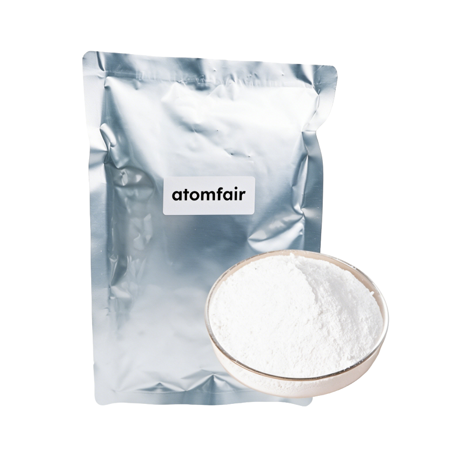
Thin-Layer Boron Nitride Nanoplates, 1-5um (SEM), <5nm (AFM), 5 gProduct Type: Shape-controlled inorganic nanomaterial
Research-grade laboratory product
|
|||||||||||||||||||||||||||||
|
|||||||||||||||||||||||||||||
|
LABORATORY PROCUREMENT SUPPORT
For model selection, material form, dimensional range, concentration or package confirmation, contact our technical sales team.
E-MAIL: inquiry@atomfair.com
|
|||||||||||||||||||||||||||||
|
Manufacturer: Atomfair LLC
Brand: ATOMFAIR®
|
Why are both SEM and AFM used to characterize lateral size and thickness of these thin-layer BN nanoplates?
SEM provides statistical lateral size distribution over large areas but cannot resolve nanometer-scale thickness; AFM measures thickness with high precision but over limited scan areas. Combining both ensures accurate morphological characterization essential for shape-controlled nanomaterials where aspect ratio is critical.
What specification parameters must be matched when integrating these h-BN nanoplates into a laboratory preparation workflow?
According to selection notes, match material form (shape-controlled inorganic nanomaterial), ingredient (h-BN), diameter (1-5 µm), thickness (<5 nm), purity (90at%), morphology (thin-layer plates), and package size (5 g) to ensure compatibility with intended preparation or comparison workflow.
What analytical infrastructure is required to verify the reported dimensions and purity of these BN nanoplates upon receipt?
To confirm diameter (1-5 µm) scanning electron microscopy (SEM) is used; thickness (<5 nm) requires atomic force microscopy (AFM); purity (90at%) is verified by energy-dispersive X-ray spectroscopy (EDS). These instruments are standard in nanomaterials characterization laboratories.
Thin-Layer Boron Nitride Nanoplates (1-5 µm lateral, <5 nm thick) offer a research-grade h-BN nanomaterial with 90 at% purity (EDS) in a 5 g package, suited for fundamental studies of thermal, mechanical, or dielectric properties in nanocomposites but limited by modest purity and small batch size.
Positive
- Ultrathin high-aspect-ratio nanoplates: The <5 nm thickness (AFM) combined with 1–5 µm lateral diameter (SEM) yields a high aspect ratio, enabling efficient thermal conductivity enhancement or mechanical reinforcement in polymer composites and coatings.
- Research-grade purity for proof-of-concept: The 90 at% purity (EDS) provides a level of chemical homogeneity sufficient for fundamental laboratory investigations, such as interfacial interaction studies or dielectric property screening.
Trade-offs
- Moderate purity limits high-end applications: At 90 at% (EDS), the material contains measurable impurities that may preclude use in applications requiring ultra-high chemical purity, such as single-photon emitters or precision electronic devices.
- Small 5 g package restricts scalability: The 5 g package size is adequate for small-scale screening or bench-top experiments but is insufficient for pilot-scale composite formulation or continuous coating trials without multiple repeat orders.
Every advanced material, component, equipment, and instrument in our catalog is backed by rigorous testing. We maintain strict internal quality management frameworks and align with CE conformity metrics to deliver transparent, reproducible performance data via our public open-science repository.
To request raw batch performance data, submit formal vendor registration paperwork, or execute a fast-turnaround R&D manufacturing loop, contact us at inquiry@atomfair.com.
Item is dispatched under the Atomfair Shipping & Delivery Framework (Free worldwide shipping on orders over $59 USD excl. heavy equipment). Return is governed by the Atomfair Return & Refund Policy (7-day technical return window).