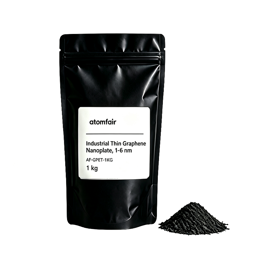
Industrial Thin Graphene Nanoplate, 1-6 nm, 1 kgProduct Type: Industrial Thin Graphene Nanoplate
Research-grade laboratory product
|
|||||||||||||||||||||||||||||
|
|||||||||||||||||||||||||||||
|
LABORATORY PROCUREMENT SUPPORT
For material selection, package confirmation, specification review or formulation-fit discussion, contact our technical sales team.
E-MAIL: inquiry@atomfair.com
|
|||||||||||||||||||||||||||||
|
Manufacturer: Atomfair LLC
Brand: ATOMFAIR®
|
Manufacturer: Atomfair LLC
Brand: ATOMFAIR®
The low bulk density (0.04-0.07 g/cm³) and tap density (0.06-0.10 g/cm³) require careful handling to prevent dusting and electrostatic charging. The user must evaluate and select appropriate storage conditions, dispersion medium, and processing route for the intended application.
- Storage Condition Evaluation: Confirm storage requirements to maintain material integrity and prevent contamination.
- Dispersion Medium Selection: Select a dispersion medium compatible with the nanoplate surface chemistry and target application.
- Processing Route Determination: Determine the processing route based on desired dispersion quality and downstream material system.
- Downstream Material Compatibility: Verify compatibility with matrix materials, binders, or solvents in the final formulation.
What conductivity and thickness specifications should be checked before using this thin graphene nanoplate in a conductive formulation?
The material is specified at 1-6 nm thickness with 800-1100 S/cm electrical conductivity, so both platelet thickness and conductivity target should be confirmed before quotation. The product is prepared by liquid-phase ultrasonic exfoliation and is positioned for conductive printing, coatings, energy materials, electronics, thermal management, composites, and sensors. Review purity, monolayer rate, surface area, density, and conductivity values where they apply to the selected formulation.
What compatibility and integration factors must be confirmed before using this graphene nanoplate in a downstream material system?
Confirm the dispersion medium, storage requirement, processing route, and downstream material system before purchase. Also confirm material family, package size, sheet or particle dimensions, thickness, functional group or conductivity target, and required quantity. The product is available as a 1 kg package with larger package options for scale-up formulation trials.
Why are bulk density and tap density important for handling this 1 kg graphene nanoplate powder?
The bulk density is 0.04-0.07 g/cm3 and tap density is 0.06-0.10 g/cm3. These low density values support packaging and feeding review, which is directly relevant to scale-up trials and 1 kg package handling. Since the material is a black powder, confirm package size and required quantity before quotation.
The Industrial Thin Graphene Nanoplate (1–6 nm, 1 kg) provides high electrical conductivity (800–1100 S/cm) and thin platelet morphology for advanced conductive formulations, but its low bulk density (0.04–0.07 g/cm³) and research-grade status necessitate careful handling and formulation validation.
Positive
- Thin platelet thickness (1–6 nm): The 1–6 nm thickness range enables formulation of conductive inks and composites requiring thinner graphene platelets, offering improved dispersion and percolation behavior in thin-film applications.
- High electrical conductivity (800–1100 S/cm): With conductivity in the 800–1100 S/cm range, this nanoplate provides a robust conductive network for energy materials, sensors, and EMI shielding, reducing filler loading requirements.
Trade-offs
- Low bulk and tap density: Bulk density of 0.04–0.07 g/cm³ and tap density of 0.06–0.10 g/cm³ present handling and feeding challenges in powder processing, requiring careful dosing equipment and dust management.
- Research-grade with formulation-fit dependency: This material is designated as research-grade; successful deployment depends on confirming dispersion medium, storage conditions, and downstream processing compatibility, which may require iterative optimization.
Every advanced material, component, equipment, and instrument in our catalog is backed by rigorous testing. We maintain strict internal quality management frameworks and align with CE conformity metrics to deliver transparent, reproducible performance data via our public open-science repository.
To request raw batch performance data, submit formal vendor registration paperwork, or execute a fast-turnaround R&D manufacturing loop, contact us at inquiry@atomfair.com.
Item is dispatched under the Atomfair Shipping & Delivery Framework (Free worldwide shipping on orders over $59 USD excl. heavy equipment). Return is governed by the Atomfair Return & Refund Policy (7-day technical return window).