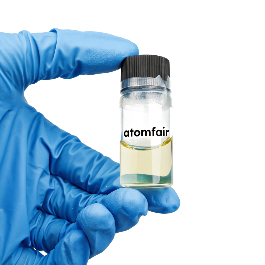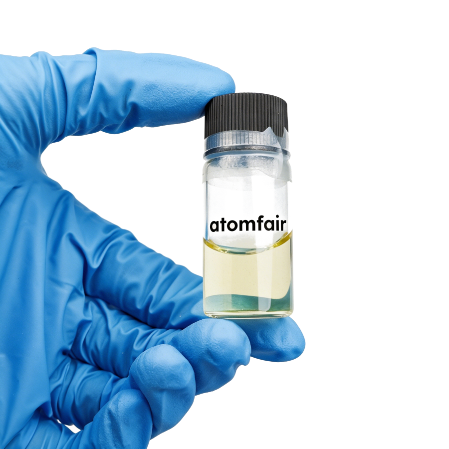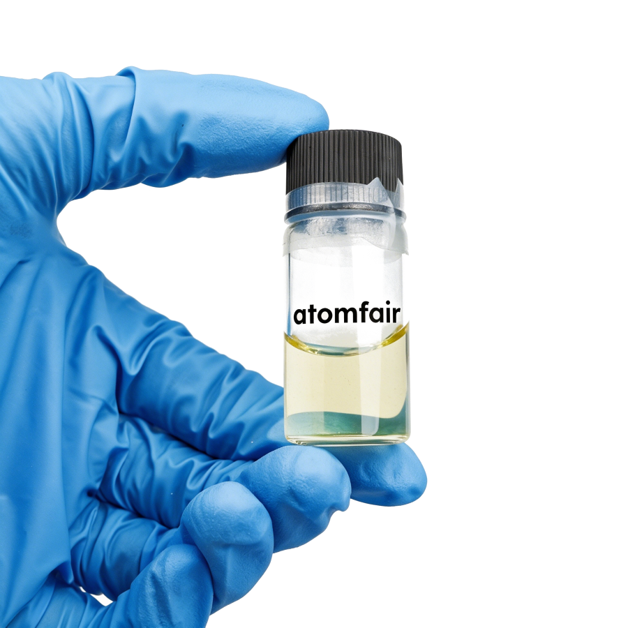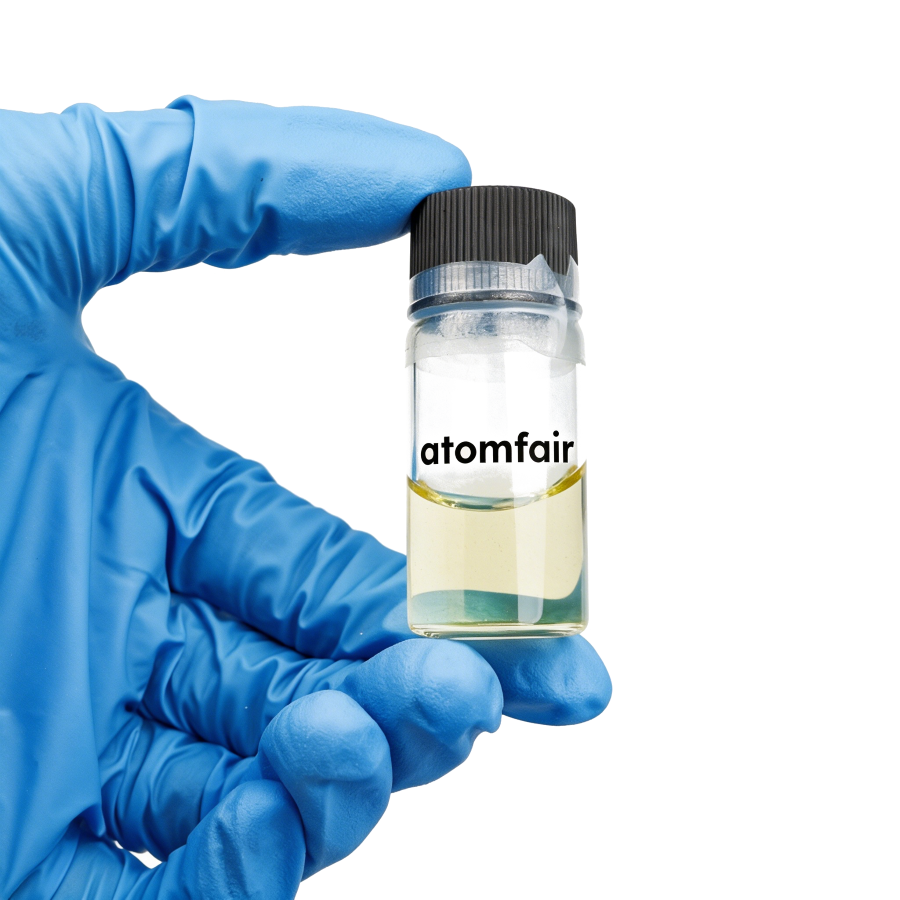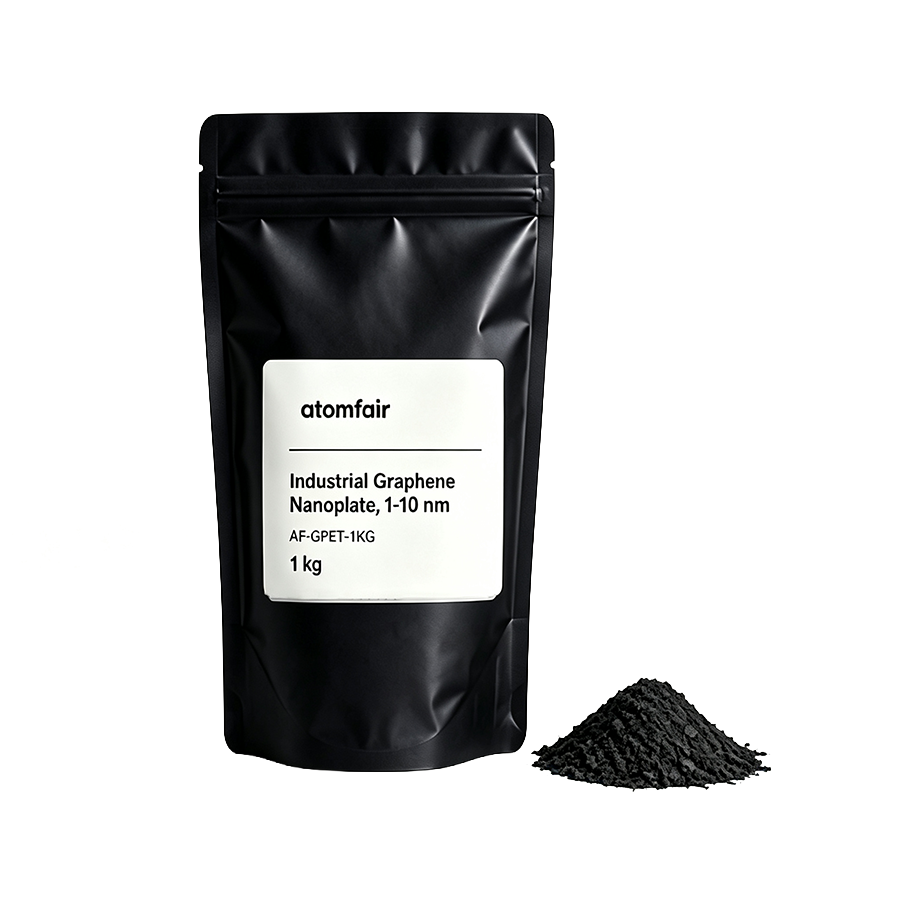
Industrial Graphene Nanoplate, 1-10 nm, 1 kgProduct Type: Industrial Graphene Nanoplate
Research-grade laboratory product
|
|||||||||||||||||||||||||||||
|
|||||||||||||||||||||||||||||
|
LABORATORY PROCUREMENT SUPPORT
For material selection, package confirmation, specification review or formulation-fit discussion, contact our technical sales team.
E-MAIL: inquiry@atomfair.com
|
|||||||||||||||||||||||||||||
|
Manufacturer: Atomfair LLC
Brand: ATOMFAIR®
|
Manufacturer: Atomfair LLC
Brand: ATOMFAIR®
What electrical conductivity range does the Atomfair AF-IGNP110-1KG industrial graphene nanoplate offer?
The specified electrical conductivity is 800-1100 S/cm, which supports conductive formulation development. The material also has a thickness range of 1-10 nm, defined as an industrial graphene nanoplate.
What are the bulk and tap density values of this graphene nanoplate, and how do they affect formulation?
Bulk density is 0.09-0.13 g/cm3 and tap density is 0.13-0.16 g/cm3. These density values are important for weighing, feeding, and formulation planning in production and research settings.
What preparation method is used for this graphene nanoplate, and what does it indicate about material quality?
The material is prepared by liquid-phase ultrasonic exfoliation, which yields a complete structure with fewer defects. This supports studies where conductivity and nanoscale platelet thickness are key selection points.
The Atomfair AF-IGNP110-1KG industrial graphene nanoplate, with 1-10 nm thickness and 800-1100 S/cm conductivity, is prepared via liquid-phase ultrasonic exfoliation yielding a black powder with bulk density 0.09-0.13 g/cm3 and tap density 0.13-0.16 g/cm3. Its defined nanoscale thickness and high conductivity support conductive formulation development, though the broad conductivity range and low bulk density require batch validation and careful handling in dry processing.
Positive
- High electrical conductivity: With 800-1100 S/cm conductivity, this graphene nanoplate enables conductive formulation development in composite and energy-material research, providing a defined performance window for electrical applications.
- Defined nanoscale platelet thickness: The 1-10 nm thickness range offers a consistent platelet dimension, supporting studies where nanoscale morphology and structure-property relationships are key selection criteria.
Trade-offs
- Conductivity range requires validation: The specified 800-1100 S/cm range is broad; applications with tight conductivity tolerances must verify batch-specific values via testing before final formulation.
- Low bulk density complicates handling: Bulk density of 0.09-0.13 g/cm3 indicates a fluffy, low-density powder that may require specialized feeding equipment or anti-dust measures during dry mixing and transfer.
Every advanced material, component, equipment, and instrument in our catalog is backed by rigorous testing. We maintain strict internal quality management frameworks and align with CE conformity metrics to deliver transparent, reproducible performance data via our public open-science repository.
To request raw batch performance data, submit formal vendor registration paperwork, or execute a fast-turnaround R&D manufacturing loop, contact us at inquiry@atomfair.com.
Item is dispatched under the Atomfair Shipping & Delivery Framework (Free worldwide shipping on orders over $59 USD excl. heavy equipment). Return is governed by the Atomfair Return & Refund Policy (7-day technical return window).