|
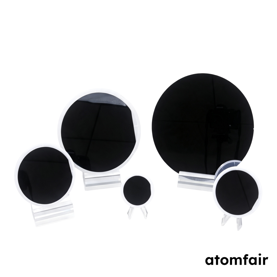
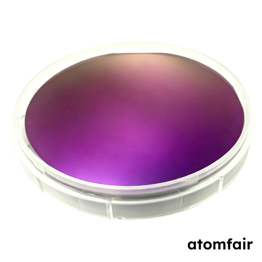
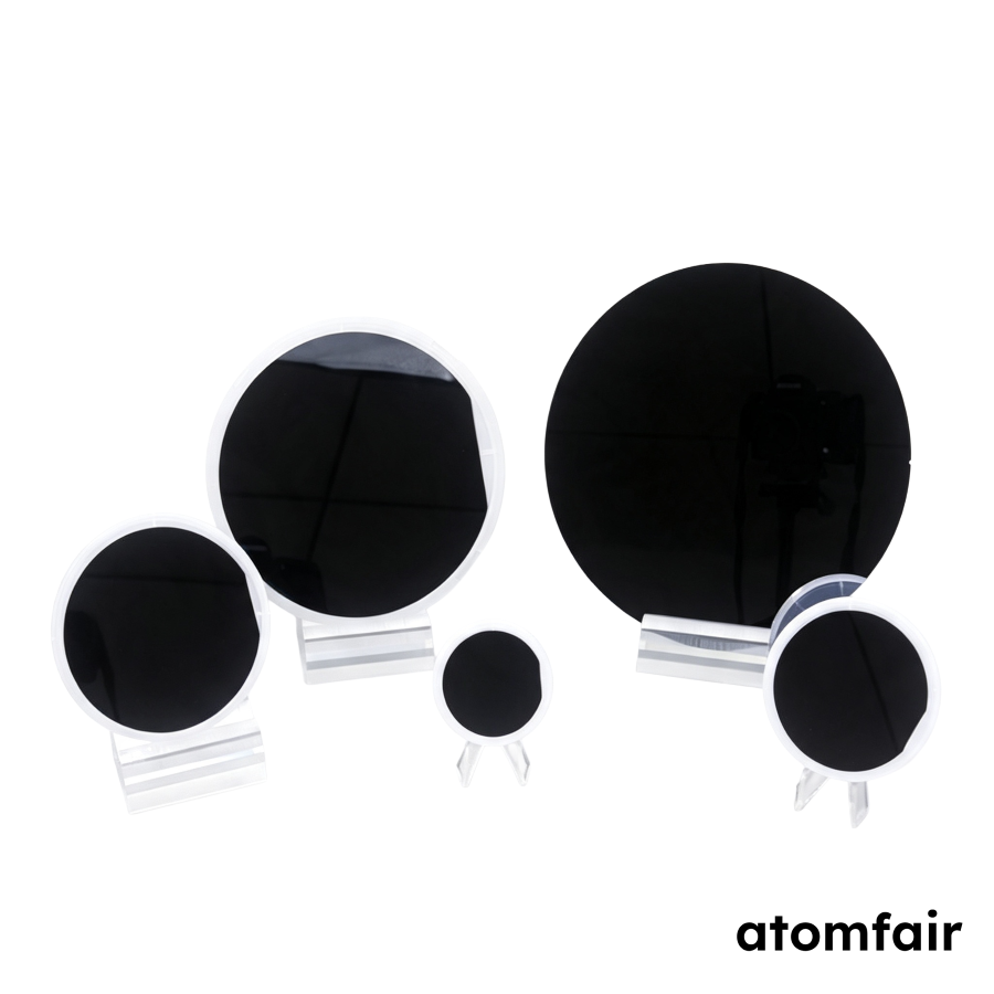
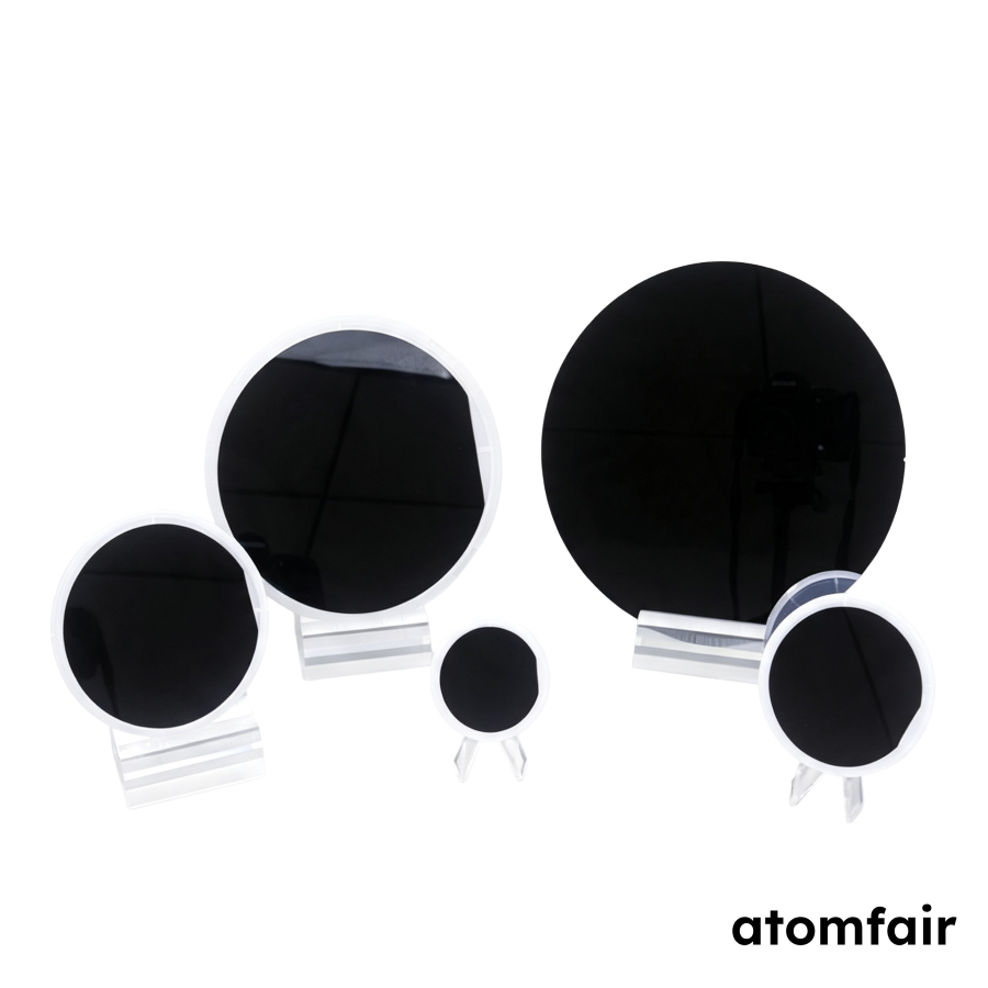
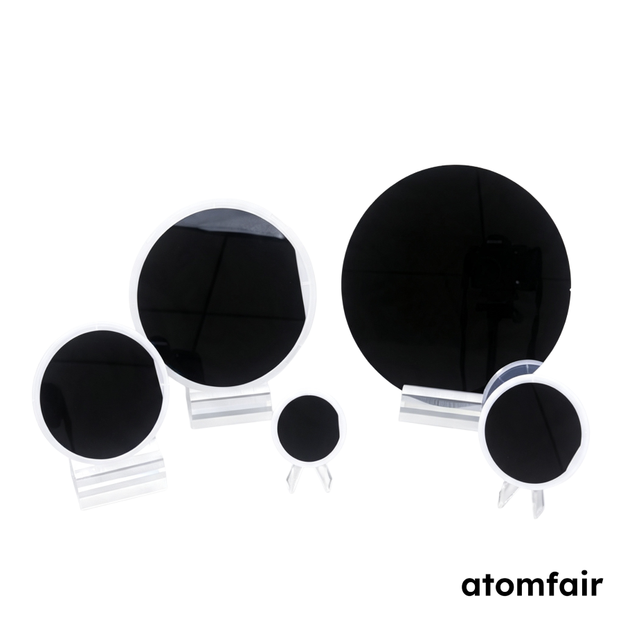
P type Monocrystalline Silicon Wafer – 2 inch (50.8 mm) <100> Single-Side Polished
Product Type: Silicon wafer
Research-grade laboratory product
|
|||||||||||||||||||||||||||||||||||
|
|||||||||||||||||||||||||||||||||||
|
PRODUCT SELECTION SUPPORT
For model selection, material matching or specification support, contact our technical sales team.
E-MAIL: inquiry@atomfair.com
|
|||||||||||||||||||||||||||||||||||
|
Manufacturer: Atomfair LLC
Brand: ATOMFAIR®
|
What are the critical dimensional and surface tolerances for the Atomfair 2-inch P-type <100> single-side polished silicon wafer?
The AF-SIW-P2100SSP is specified with a typical thickness of 400 +/- 25 um, TTV <5 um, BOW <10 um, WARP <10 um, and front-side roughness Ra <0.5 nm. These tolerances apply to the 2-inch (50.8 mm) wafer format and are relevant for lithography, bonding, or thin-film process planning. The back side is etched.
Can this 2-inch P-type <100> wafer be configured for double-side polishing instead of single-side polishing?
Yes; the surface finish is selected as either SSP or DSP, and the backside condition is specified separately. The standard AF-SIW-P2100SSP configuration is single-side polished with an etched back side, but DSP is available by selecting the surface requirement at ordering. The polished front-side roughness is Ra <0.5 nm.
Which resistivity range should be selected for this P-type silicon wafer, and what options are available?
Resistivity is a selectable specification: 0.001-0.005 ohm.cm, 1-10 ohm.cm, >10 ohm.cm, >5K ohm.cm, or >10K ohm.cm. The final resistivity requirement must be provided when ordering the 2-inch P-type <100> SSP wafer. The material is 6N monocrystalline silicon available in CZ or FZ form.
Two-inch <100> P-type monocrystalline silicon wafer with single-side polished finish, 400 µm thickness, and sub-0.5 nm front-side roughness. Offers tight geometric tolerances (TTV <5 µm, BOW/WARP <10 µm) and selectable resistivity from 0.001 to >10K ohm.cm, making it suitable for research-grade semiconductor device fabrication and thin-film deposition processes.
Positive
- High surface quality: Front-side roughness Ra <0.5 nm enables precise epitaxial growth or thin-film deposition with minimal scattering or defect nucleation.
- Tight geometric tolerances: TTV <5 um, BOW <10 um, and WARP <10 um ensure uniform substrate flatness critical for photolithography alignment and wafer bonding processes.
Trade-offs
- Handling sensitivity: Single-side polished finish with etched back side requires cleanroom-grade handling and storage to avoid scratches or particulate contamination on the active surface.
- Resistivity selection required: Multiple resistivity options demand accurate specification based on device design; mismatched resistivity can alter carrier mobility or junction characteristics.
Every advanced material, component, equipment, and instrument in our catalog is backed by rigorous testing. We maintain strict internal quality management frameworks and align with CE conformity metrics to deliver transparent, reproducible performance data via our public open-science repository.
To request raw batch performance data, submit formal vendor registration paperwork, or execute a fast-turnaround R&D manufacturing loop, contact us at inquiry@atomfair.com.
Item is dispatched under the Atomfair Shipping & Delivery Framework (Free worldwide shipping on orders over $59 USD excl. heavy equipment). Return is governed by the Atomfair Return & Refund Policy (7-day technical return window).