|
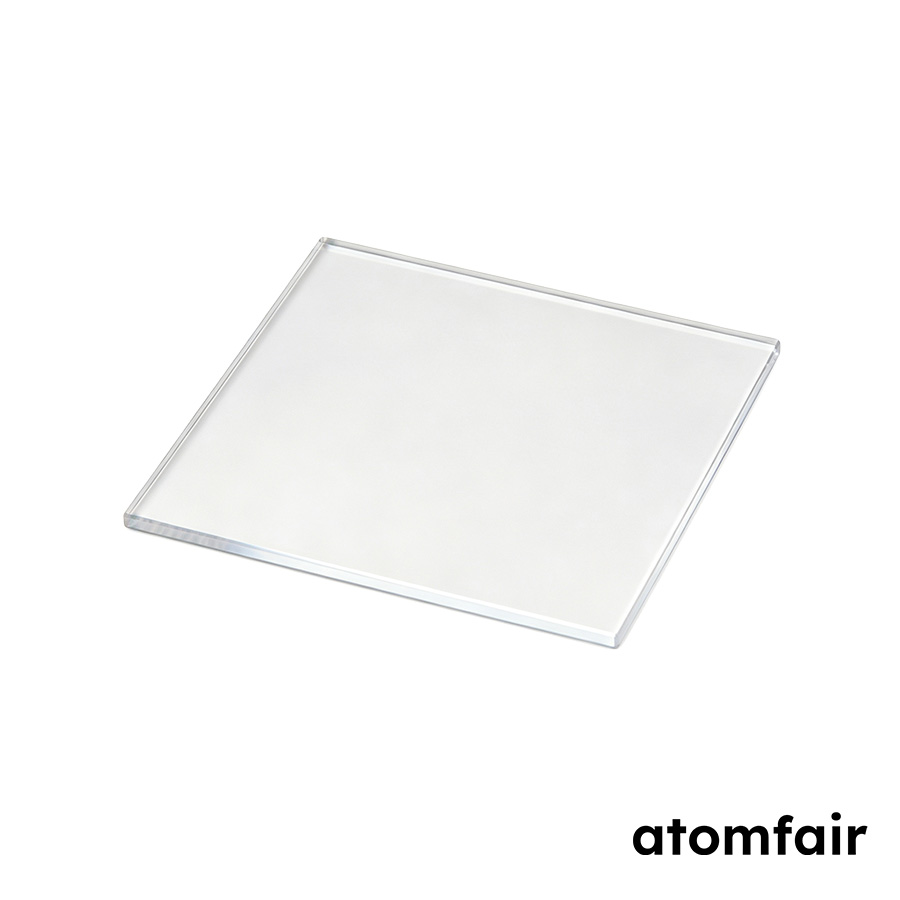
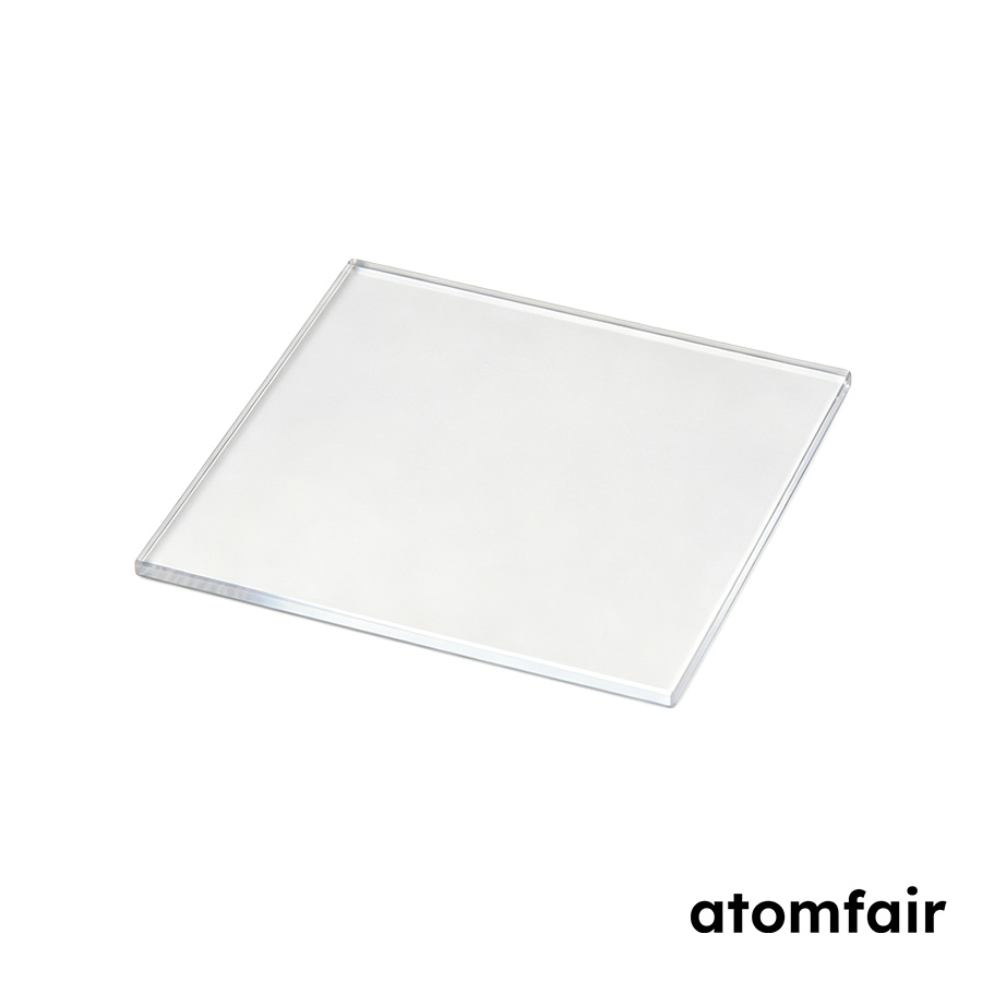
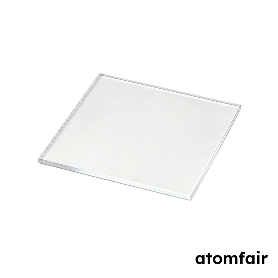
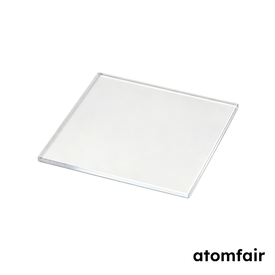
Lithium Niobate (LiNbO3) Crystal Substrate, 5 × 5 × 0.5 mm, (10-10), single-side polished (10 Pieces per Box)
Product Type: Lithium niobate crystal substrate
Research-grade laboratory product
|
|||||||||||||||||||||||||||||||||||||||||||
|
|||||||||||||||||||||||||||||||||||||||||||
|
LABORATORY PROCUREMENT SUPPORT
For model selection, coating review, platform compatibility or configuration confirmation, contact our technical sales team.
E-MAIL: inquiry@atomfair.com
|
|||||||||||||||||||||||||||||||||||||||||||
|
Manufacturer: Atomfair LLC
Brand: ATOMFAIR®
|
This document outlines the technical constraints for handling the Atomfair lithium niobate crystal substrate. The substrate is sensitive to surface contamination and mechanical damage, requiring careful handling and storage.
- Surface Integrity Constraint: The polished surface must be protected from contact with particulates or abrasive materials to maintain the specified surface roughness of less than 5 Å.
- Environmental Sensitivity: The substrate should be stored in a clean, dry environment to prevent surface contamination or moisture adsorption that could affect optical performance.
- Orientation Verification: The crystallographic orientation tolerance of less than 0.5° must be verified before use in critical optical applications.
This procedure describes the safe handling and preparation of the lithium niobate crystal substrate for optical or electro-optic device integration. Proper handling is essential to preserve surface quality and prevent damage.
Required Equipment: Cleanroom-grade gloves, Vacuum tweezers, Cleanroom wipes
- Inspect the substrate
Inspect the substrate for any visible damage or contamination upon removal from its packaging. - Handle with clean tools
Handle the substrate using cleanroom-grade gloves or vacuum tweezers to avoid direct contact with the polished surface. - Clean the surface if necessary
Clean the substrate surface with a cleanroom wipe and an appropriate solvent if any particulate contamination is observed. - Store in a protective container
Store the substrate in a clean, dry, and protective container when not in use to prevent environmental damage.
What are the practical differences between single-side polished and double-side polished LiNbO3 substrates for nonlinear optical device fabrication?
Single-side polished substrates, like this 5×5×0.5 mm (10-10) variant, provide one optically smooth surface (roughness <5 Å) suitable for applications where only one side requires optical quality, such as when the substrate is mounted or bonded. The product description lists double-side polishing as a routine processing option, indicating that both surfaces can be polished to <5 Å roughness if required. For devices like optical modulators or waveguides that need both surfaces optically flat, double-side polished substrates are recommended.
How does the (10-10) orientation of this LiNbO3 substrate compare to (0001) and (11-20) orientations for electro-optic applications?
The (10-10) orientation is one of three routine orientations offered, alongside (0001) and (11-20). The electro-optic coefficients (γ13=9, γ22=3.4, γ33=31 pm/V) are material constants, but the effective electro-optic response depends on the crystal orientation relative to the applied field. The orientation tolerance is <0.5°, ensuring precise alignment. For specific device geometries, the optimal orientation may vary; technical support can assist in selection.
Is this LiNbO3 substrate MgO-doped, and what is the impact of MgO doping on optical damage threshold?
This specific product is not described as MgO-doped; it is listed as nonlinear optical grade LiNbO3. The product description notes that MgO doping is a method to improve optical damage threshold, which is critical for high-power applications such as frequency doubling or parametric oscillators. If a higher damage threshold is required, MgO-doped variants should be requested during quotation.
This Atomfair 5×5×0.5 mm LiNbO3 substrate with (10-10) orientation and single-side polish provides high nonlinear optical coefficients and broad spectral transmission for nonlinear and electro-optic applications, but the single-side polish and fixed orientation impose constraints on experimental flexibility.
Positive
- High nonlinear optical coefficients: With d33 = 34.45 pm/V, d31 = d15 = 5.95 pm/V, and d22 = 13.07 pm/V, this substrate enables efficient frequency doubling and parametric oscillation.
- Broad spectral transmission: Transmission from 0.4 to 2.90 μm covers visible and near-infrared wavelengths, suitable for a wide range of nonlinear and electro-optic applications.
Trade-offs
- Single-side polished surface: Provided with single-side polish only, which may not meet the requirements of applications that need double-side polished surfaces for optical path symmetry or interferometric setups.
- Fixed (10-10) orientation: This substrate is cut to a single (10-10) orientation, restricting its use to applications that require that specific plane; other orientations are not available in this product variant.
Every advanced material, component, equipment, and instrument in our catalog is backed by rigorous testing. We maintain strict internal quality management frameworks and align with CE conformity metrics to deliver transparent, reproducible performance data via our public open-science repository.
To request raw batch performance data, submit formal vendor registration paperwork, or execute a fast-turnaround R&D manufacturing loop, contact us at inquiry@atomfair.com.
Item is dispatched under the Atomfair Shipping & Delivery Framework (Free worldwide shipping on orders over $59 USD excl. heavy equipment). Return is governed by the Atomfair Return & Refund Policy (7-day technical return window).