Description
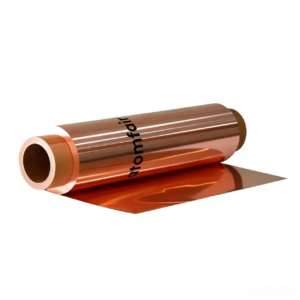
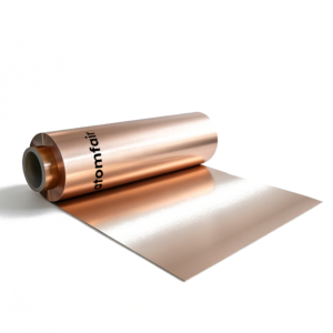
ATOMFAIR® TREATED RA COPPER FOILRESEARCH GRADE MATERIAL
|
|||||||||||||||||||||||||||||||||||||||||
|
|||||||||||||||||||||||||||||||||||||||||
|
TAILORED SOLUTIONS FOR RESEARCH
Contact our engineering team for technical support or official institutional quotations.
EMAIL: inquiry@atomfair.com
|
|||||||||||||||||||||||||||||||||||||||||
|
Manufacturer: Atomfair LLC
Brand: ATOMFAIR®
|
|||||||||||||||||||||||||||||||||||||||||
This document describes the critical handling and environmental constraints for Atomfair treated RA copper foil to preserve its functional performance. The foil's single-sided roughened surface and anti-oxidation coating require clean handling, careful mechanical use, and proper thermal processing to maintain adhesion, cleanliness, and bending durability.
- Cleanliness Maintenance: Store and handle the foil in a clean environment equivalent to Class 1000–10000 to prevent particle contamination that could impact circuit printing and adhesion.
- Surface Integrity: Avoid mechanical abrasion or contact that may dislodge copper buds or cause powder shedding from the roughened surface.
- Thermal Processing Compatibility: Use lamination or soldering profiles that do not exceed the anti-oxidation treatment's thermal stability to avoid discoloration or conductive degradation.
- Bending Fatigue Limits: Do not exceed 10,000 repeated bending cycles at 180° to prevent cracking and ensure long-term structural integrity.
What are the performance trade-offs between reddening and blackening treatments on Atomfair Treated RA Copper Foil for FCCL applications?
Reddening treatment uses copper powder (red surface) and minimizes contamination risk due to the copper-only chemistry, while blackening treatment uses cobalt-nickel powder (black surface) and provides different adhesion characteristics for specific laminate chemistries. Both treatments undergo single-sided roughening and high-temperature anti-oxidation to prevent discoloration during processing, with no powder shedding from uniform copper buds. The choice depends on the required peel strength profile and compatibility with the FCCL resin system.
Can Atomfair Treated RA Copper Foil support ultra-fine line FPC designs below 30 μm line width and spacing?
Yes, the foil supports minimum line width and spacing of 30 μm/30 μm, as enabled by its stable thickness tolerance of ±3% of nominal thickness and uniform copper buds with no powder shedding. These properties ensure circuit printing accuracy and reliability for fine-line FPC production compliant with IPC-4101 specifications.
What storage and handling conditions are required to preserve the anti-oxidation and cleanliness properties of Atomfair Treated RA Copper Foil?
The foil must be stored in its original dust-free packaging to maintain the cleanliness level achieved in the ISO 14644-1 compliant Class 1000-10000 cleanroom, with particle count ≤5 particles/100cm² for particles ≥5 μm. Handling should use clean gloves to avoid contaminating the high-temperature anti-oxidation layer, which prevents discoloration during processing. Avoid exposure to high humidity or corrosive environments to preserve the treated surface integrity.
Atomfair Custom Treated RA Copper Foil provides single-sided roughening that enhances composite peel strength and high bending resistance (10,000+ cycles), ideal for flexible circuits and fine-line FPC; however, its single-sided treatment limits two-sided adhesion, and strict handling procedures are required to preserve its high cleanliness specification.
Positive
- Single-sided roughening for peel strength: The single-sided roughening treatment creates a matte surface with uniform copper buds that enhances adhesion with composite materials, preventing peeling in FCCL and FPC applications.
- High bending resistance (10,000+ cycles): The foil passes repeated bending tests up to 10,000 cycles at 180° without cracking, ensuring durability in flexible circuits and foldable electronic devices.
Trade-offs
- Single-sided adhesion limitation: Only one side is roughened; the opposite smooth side may not provide adequate peel strength for double-sided bonding applications.
- Cleanliness requires controlled handling: Produced in a Class 1000-10000 dust-free workshop, the foil's particle count specification (≤5 particles/100cm² for ≥5μm) necessitates careful storage and handling to avoid contamination.
Every advanced material, component, equipment, and instrument in our catalog is backed by rigorous testing. We maintain strict internal quality management frameworks and align with CE conformity metrics to deliver transparent, reproducible performance data via our public open-science repository.
To request raw batch performance data, submit formal vendor registration paperwork, or execute a fast-turnaround R&D manufacturing loop, contact us at inquiry@atomfair.com.
Item is dispatched under the Atomfair Shipping & Delivery Framework (Free worldwide shipping on orders over $59 USD). Return is governed by the Atomfair Return & Refund Policy (7-day technical return window).