Description
ATOMFAIR® GRAPHENE NANOPLATELETSRESEARCH GRADE MATERIAL
|
||||||||||||||||||||||||
|
||||||||||||||||||||||||
|
|||
|
TAILORED SOLUTIONS FOR RESEARCH
Contact our engineering team for technical support or official institutional quotations. Use our high-quality materials to elevate your experimental performance!
EMAIL: info@atomfair.com
|
|||
|
Manufacturer: Atomfair LLC
Brand: ATOMFAIR®
|
Graphene nanoplatelets require verification of thickness and lateral dimensions using electron or atomic force microscopy. The high surface area of the material necessitates controlled dispersion techniques to prevent agglomeration in composite formulations.
- Characterization Requirement: Characterize the nanoplatelets using atomic force microscopy (AFM), transmission electron microscopy (TEM), or scanning electron microscopy (SEM) to confirm thickness and diameter.
How does the thickness range of 1-10 nm affect the balance between surface area and mechanical reinforcement in composites?
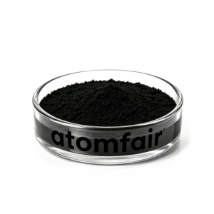
The graphene nanoplatelets have a thickness of 1-10 nm and are described as having high surface area for enhanced reactivity and mechanical strength for improved durability in composites. Thinner platelets within this range increase surface area and interfacial bonding, leading to stronger reinforcement, whereas thicker platelets may reduce surface area but improve handling and dispersion. The product is explicitly designed for composite applications, and the 1-10 nm range is intended to balance these performance factors.
Can these graphene nanoplatelets be used directly in solvent-based coating formulations without additional functionalization?
Yes, the nanoplatelets are intended for use in coatings and can be incorporated into solvent-based systems without stated need for functionalization, as they are produced by CVD, liquid-phase exfoliation, or mechanical milling — all methods that yield pristine surfaces compatible with organic solvents. However, storage instructions require a cool, dry place away from moisture, indicating sensitivity to water, so water-based formulations may require additional dispersion agents or stability testing.
What specific storage and handling infrastructure is needed to maintain the integrity of these graphene nanoplatelets?
The product must be stored in a cool, dry place away from direct sunlight and moisture to prevent degradation. Appropriate personal protective equipment (PPE) must be used during handling, and disposal must follow local regulations for nanomaterials. No inert atmosphere or refrigerated storage is specified; standard laboratory conditions with controlled humidity and temperature are sufficient based on the provided guidelines.
ATOMFAIR Graphene Nanoplatelets provide high surface area and electrical conductivity suitable for composites and electronics research, yet require controlled storage to prevent moisture-induced agglomeration and demand strict nanomaterial handling protocols for safe laboratory use.
Positive
- High Surface Area: Provides enhanced reactivity and performance in composites, enabling more efficient interfacial interactions between filler and matrix.
- Outstanding Electrical Conductivity: Ideal for electronics and energy storage applications, improving device efficiency and power density by reducing resistance.
Trade-offs
- Controlled Storage Required: Must be stored in a cool, dry place away from direct sunlight and moisture to prevent degradation, agglomeration, or loss of functional properties.
- Nanomaterial Handling Precautions: Requires appropriate PPE and disposal per local regulations for nanomaterials to mitigate inhalation risk and environmental contamination.
Every advanced material, component, equipment, and instrument in our catalog is backed by rigorous testing. We maintain strict internal quality management frameworks and align with CE conformity metrics to deliver transparent, reproducible performance data via our public open-science repository.
To request raw batch performance data, submit formal vendor registration paperwork, or execute a fast-turnaround R&D manufacturing loop, contact us at inquiry@atomfair.com.
Item is dispatched under the Atomfair Shipping & Delivery Framework (Free worldwide shipping on orders over $59 USD). Return is governed by the Atomfair Return & Refund Policy (7-day technical return window).