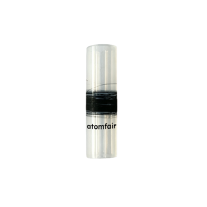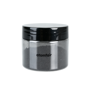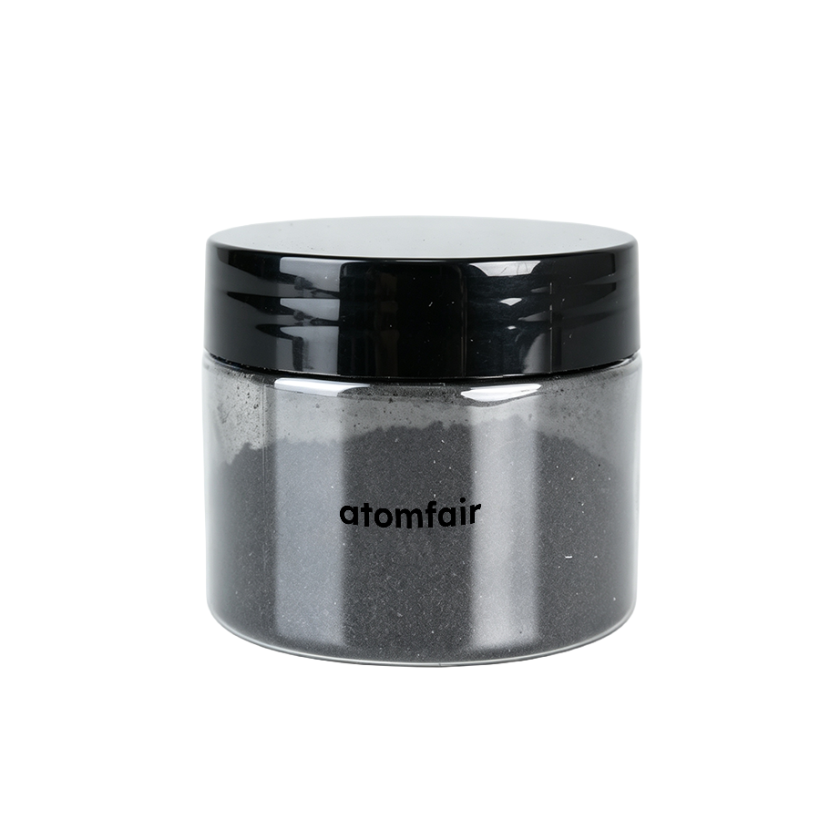
Industrial-gradesingle-walled carbon nanotubes, OD 1-2 nm(TEM), length 10-30um(SEM), purity ~95 wt%(EDS)Product Type: Single-walled carbon nanotube material
Research-grade laboratory product
|
|||||||||||||||||||||||
|
|||||||||||||||||||||||
|
LABORATORY PROCUREMENT SUPPORT
For model selection, material specification matching, application fit or quotation confirmation, contact our technical sales team.
E-MAIL: inquiry@atomfair.com
|
|||||||||||||||||||||||
|
Supplier: Atomfair
Brand: ATOMFAIR®
|
Manufacturer: Atomfair LLC
Brand: ATOMFAIR®
Why are the diameter and length of the AF-SWCNT-S31 measured by different techniques (TEM vs. SEM), and what does this reveal about the material's dimensional uniformity?
The diameter is measured by TEM (1-2 nm) because TEM provides nanoscale resolution, while length is measured by SEM (10-30 μm) due to its larger field of view. This combination indicates that the material is characterized across multiple length scales, but the source does not provide quantitative uniformity data beyond the specified ranges.
How does the ~95 wt% purity (EDS) of the AF-SWCNT-S31 affect its suitability for sensitive electrochemical sensor applications?
The purity of ~95 wt% as measured by EDS indicates a relatively low level of impurities, which is beneficial for minimizing background signals in electrochemical sensors. However, the source does not specify the chemical nature of the remaining 5%, so further characterization may be required for absolute compatibility with sensitive sensor platforms.
What information must be confirmed before procurement of the AF-SWCNT-S31 to ensure proper handling and integration into a research workflow?
The source specifies that before quotation, one must confirm nanotube wall type, outer diameter, length, purity, functional group, and package size. This ensures that the material matches the intended application and that appropriate handling procedures can be established based on the exact specifications.
This industrial-grade single-walled carbon nanotube material (model AF-SWCNT-S31) offers an outer diameter of 1–2 nm (TEM), length of 10–30 μm (SEM), and purity of ~95 wt% (EDS), with a specific surface area of ~1380 m²/g, making it suitable for dispersion, composite, electrode, and conductivity research workflows.
Positive
- High specific surface area: A specific surface area of ~1380 m²/g provides extensive active sites for adsorption, catalysis, or electrode applications, enhancing interfacial interactions in composite or energy storage systems.
- Narrow diameter distribution: The 1–2 nm outer diameter (TEM) ensures consistent electronic and mechanical properties across the batch, critical for reproducible nanotube-based device fabrication or formulation.
Trade-offs
- Handling sensitivity of dry powder: As a black powder with high surface area, the material is prone to electrostatic charging and airborne dispersion, requiring careful handling in a fume hood or glovebox to avoid inhalation and contamination.
- Purity verification needed per batch: The stated purity of ~95 wt% (EDS) may vary between batches; buyers should confirm the actual purity via their own analysis for applications where trace metal or carbonaceous impurities affect performance.
Every advanced material, component, equipment, and instrument in our catalog is backed by rigorous testing. We maintain strict internal quality management frameworks and align with CE conformity metrics to deliver transparent, reproducible performance data via our public open-science repository.
To request raw batch performance data, submit formal vendor registration paperwork, or execute a fast-turnaround R&D manufacturing loop, contact us at inquiry@atomfair.com.
Item is dispatched under the Atomfair Shipping & Delivery Framework (Free worldwide shipping on orders over $59 USD excl. heavy equipment). Return is governed by the Atomfair Return & Refund Policy (7-day technical return window).