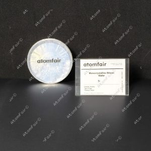
Description
| Properties | Specification |
|---|---|
| Diameter | 4″ |
| Thickness | 500 μm |
| Type | P |
| Doping | Boron |
| Orientation | 7° off <100> |
| Resistivity | 1–40 Ω·cm |
| Surface | Single / Double‑side polished |
| Reference Edge | Yes |
Every advanced material, component, equipment, and instrument in our catalog is backed by rigorous testing. We maintain strict internal quality management frameworks and align with CE conformity metrics to deliver transparent, reproducible performance data via our public open-science repository.
To request raw batch performance data, submit formal vendor registration paperwork, or execute a fast-turnaround R&D manufacturing loop, contact us at inquiry@atomfair.com.
Item is dispatched under the Atomfair Shipping & Delivery Framework (Free worldwide shipping on orders over $59 USD). Return is governed by the Atomfair Return & Refund Policy (7-day technical return window).